
PCBスタックアップ
PCBスタックアップとは?
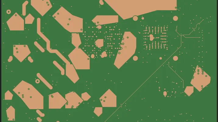
PCBスタックアップは、複数層PCB内の各層の厚さ、材質、および構成を定義します。スタックアップはインピーダンス、信号伝播遅延、および熱特性を直接影響させます。スタックアップは、銅層(信号およびパワー)と誘電体層(プリプレグおよびコア)のシーケンスです。
PCBスタックアップは、複数層PCB内の各層の厚さ、材質、および構成を定義します。スタックアップはインピーダンス、信号伝播遅延、および熱特性を直接影響させます。スタックアップは、銅層(信号およびパワー)と誘電体層(プリプレグおよびコア)のシーケンスです。