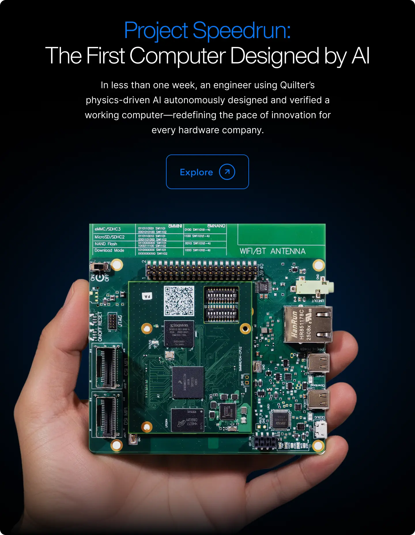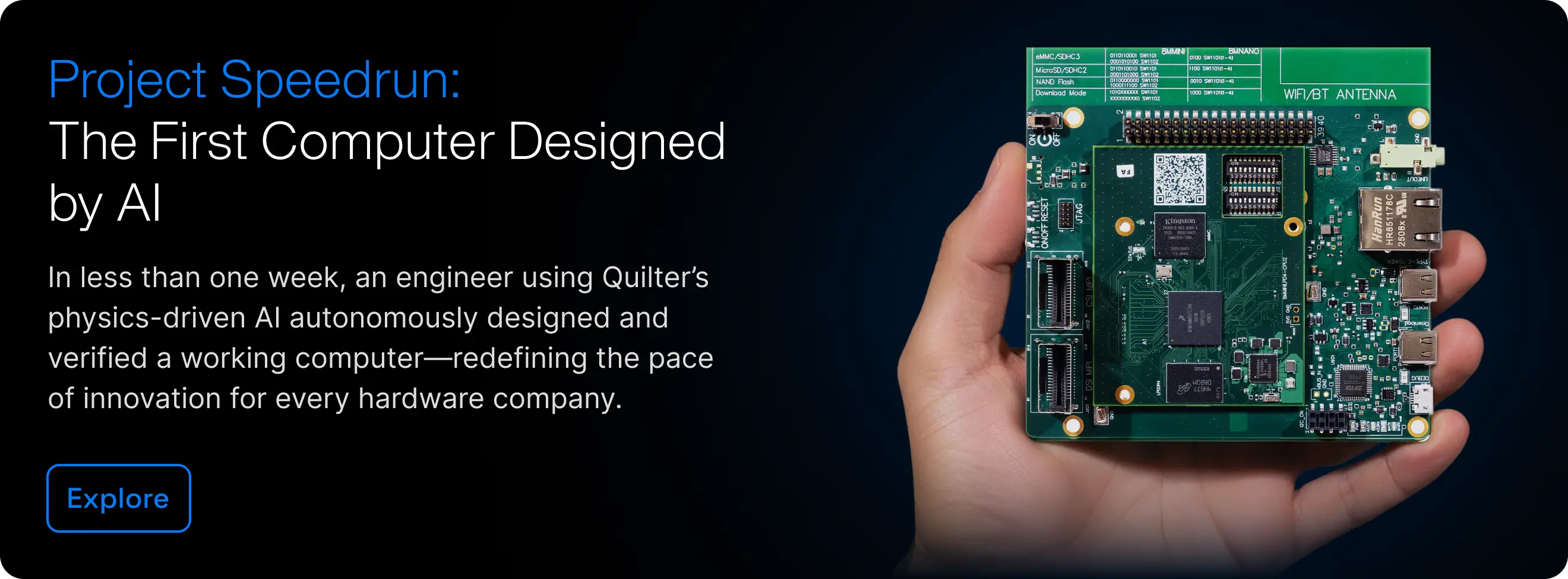
PCBレイアウトを自動化する物理法則に基づくAI

Quilterは、PCBの部品配置と配線を自動化する、物理法則に基づくAIです。

信頼される業界パートナー:

AWS, a Quilter industry partner
NVIDIA, a Quilter industry partner
Siemens, a Quilter industry partner

プロジェクトをQuilterにアップロードすると何が起こるか

1

手作業のレイアウトとQuilterによるレイアウト自動化の比較

専門家が428時間と見積もったレイアウト作業が、Quilterでは38.5時間の手作業による仕上げで完了しました。

Before: Manual Layout
Mon
Tue
Wed
Thu
Fri
Sat
Sun
n0
Start Working on Layout
Layout in Progress
n1
Layout in Progress
n2
Layout in Progress
n3
Layout in Progress
Engineer Reviews Draft and Requests Changes
Layout in Progress
n4
Layout in Progress
Engineer Reviews Final Layout
Submit to Fab
Fabrication and Assembly
n5
Fabrication and Assembly
Board Arrives
After: Layout with Quilter
Mon
Tue
Wed
Thu
Fri
Sat
Sun
n0
Submit to Quilter
Quilter Generates 100s of Candidates
n1
Engineer Reviews Candidates and Makes Adjustments
Submit to Fab
Fabrication and Assembly
n2
Fabrication and Assembly
Board Arrives

チームがQuilterを選ぶ理由

増員せずに開発規模を拡大

人員を増やさず、より多くの基板を開発できます。レイアウトの専門人材は不足しており、設計は担当者の空きを待つことになります。Quilterは複数の基板を夜間に並行処理するため、今のチームで未処理の設計を進められます。

納期を短縮

4〜8週間かかっていた基板が、数日で仕上がります。ファームウェアチームの待ち時間がなくなり、検証を早く始められます。従来1回にかかっていた時間で、2回または3回の反復設計を行えます。

ハードウェアで実績のあるAI

企業のAI試験導入の多くは、概念実証の段階で停滞します。一方、民生用電子機器、航空宇宙、防衛分野のハードウェアチームは、Quilterを使って、実際に製造へ進む基板をすでに設計しています。

主要なECAD形式をすべてネイティブにサポート

Cadence ECAD format supported by Quilter
Altium Designer supported by Quilter
KiCad ECAD format supported by Quilter
OrCAD ECAD format supported by Quilter
Siemens Xpedition ECAD format supported by Quilter

How Quilter Works

ECAD Quilter Prepare Your Design Files Schematic Board Outline Fixed Components Edit & Clean Up Design Review Iteration Loop Define Design Context Stackup Constraints Circuit Intent Review Candidates Placement Routing Quilter Engine

Quilter fits into your existing workflow. You prepare the design in your ECAD, upload it, and Quilter handles placement and routing. You review the output, make adjustments, and resubmit. Most boards go through 2 to 5 cycles before the engineer is satisfied with the result. There’s no magic: Quilter shows you every physics check it ran, and you stay in control at every step.

Explore How Quilter Works

How Quilter Works

ECAD Quilter Prepare Your Design Files Schematic Board Outline Fixed Components Tweak Placement Final Cleanup Design Review Iteration Loop Define Design Context Stackup Constraints Circuit Intent Review Placement Review Routing Quilter Engine

Quilter fits into your existing workflow. You prepare the design in your ECAD, upload it, and Quilter handles placement and routing. You review the output, make adjustments, and resubmit. Most boards go through 2 to 5 cycles before the engineer is satisfied with the result. There’s no magic: Quilter shows you every physics check it ran, and you stay in control at every step.

Explore How Quilter Works

Tony Fadell headshot

Quilterは優れたPCB設計者に、数週間を数日に変える力を与えます。これはパラダイムの抜本的な転換です。反復設計を速めれば、競合より速くイノベーションを生み出せます。

Tony Fadell

Build Collectiveプリンシパル、「iPodの父」、iPhone共同発明者、Nest創業者

「長年回路設計を手がけてきた人なら、最初は疑い、単なる高機能なオートルーターだと思うでしょう。オートルーティングを試して気に入った人はいなかったからです。しかし、皆さんの部品配置へのアプローチは、その多くの障壁を乗り越え、時間を節約できる本当に役立つツールにしています。」

プリンシパルエンジニア、防衛・航空宇宙分野

「最大の価値は効率です。基本設計の派生版を短期間で作るには、多くの労力がかかります。Quilterを使えば、これまでよりはるかに速く、より多くのお客様に対応できます。」

部門責任者、半導体業界

新たなオートルーターを作ったのではありません

オートルーターの発想は正しかったのです。ただ、技術が追いついていませんでした。基礎的な物理法則に基づいて学習した強化学習が、その状況を変えます。Quilterは単にネットを接続するだけでなく、回路の電気的な振る舞いを考慮した基板をコンパイルします。

1960年代

マイラーフィルムとテープ

手作業で切り貼り

1980年代

CADレイアウト

作図のデジタル化

2000年代

オートルーター

幾何形状のみ

現在

物理法則に基づくAI

基板全体のコンパイル

配線には、すべてのネットを接続し、すべてのルールを守るという明確な目標があります。部品配置はそうではありません。適切な配置とは配線可能な配置であり、それは試してみなければ分かりません。

Quilterは、同じ物理法則に基づき、配置と配線を一つの問題として解きます。

Quilterとオートルーターの違いを詳しく見る。

規制の厳しい業界と現代の知的財産保護要件に対応

お客様のデータを学習に使用しません

多くのAIツールの性能は、与えられるデータの質に左右されます。そのため、価値を生み出す前に停滞してしまう例も少なくありません。Quilterは、AlphaGoが囲碁を学んだように、数百万もの合成基板を物理法則に照らして試行し、レイアウトを学びました。お客様のデータで学習することはありません。大規模なデータ整備プロジェクトを経ずに、最初の基板から価値を得られます。

サイバーセキュリティのベストプラクティスに準拠

データは、セキュリティのベストプラクティス(TLS1.3、AES-256)に従い、保存時と転送時に暗号化されます。独立した監査を受け、業界標準に準拠しています。SOC 2 Type IIがお客様の設計データに意味すること↗

自社環境への導入に対応

お客様のインフラ内にQuilterを導入する選択肢をご用意しています。アクセス、ネットワーク、データの保存場所はお客様が管理し、アプリケーションは当社が管理します。

Diagram of Quilter IP protection and data isolation

Quilterが得意とする領域

Quilterには現在、特に適した設計領域があり、製品の更新ごとにその範囲が広がっています。多くのチームは、Quilterが得意とする基板では工程全体を任せ、より複雑な基板では重要な部分を自ら事前配線し、定型的な部分をQuilterに任せています。急速に進化するツールを使いこなすために、今から経験を積み始めましょう。

Dimension Current Capabilities Status
Components 100 to 1,000 per board Live
Pins to route No inherent limit, but the current best performance is around 2000-5000 Live
Pin density Under 20% Pin density (%) = (Component Pin Area) / (Total Board Surface Area) × 100% Live
Via types Through-hole vias Live
Blind & buried vias In development
BGA fanouts Automated fanout generation Beta
Length matching Coming soon In development
RF Pre-route RF nets, Quilter can handle the rest In development