
製造性設計(DFM)
製造性設計(DFM)とは?
製造性設計(DFM)は、PCBがプロセス内で正常に製造、組立、および実装テストできることを保証するガイドライン、ルール、およびベストプラクティスの集合です。DFM考慮事項には、対象製造施設で実現可能な最小トレース幅と間隔、ビアドリルサイズとアスペクト比、はんだマスクとシルクスクリーンクリアランス、リフロー又はウェーブはんだ付けに最適化されたパッドジオメトリ、自動ピック・アンド・プレース機械のコンポーネント間隔、およびIn-Circuit Testing (ICT) または自動光学検査(AOI)のテストポイントアクセシビリティが含まれます。
設計段階中にDFMを無視すると、製造イール問題、生産コスト増加、および市場投入時間の遅延が生じます。DFM違反の一般的な例には、選択された銅厚に対して薄すぎるトレース、ファブハウスの能力を超えるアスペクト比のビア、はんだブリッジリスクのためのコンポーネント間の不十分なクリアランス、およびトンボストーン傾向のあるパッド設計があります。これらの問題は、製造ツーリングが作成された後で修正する方が非常に高くつきます。
AI搭載PCBレイアウトへのDFM統合
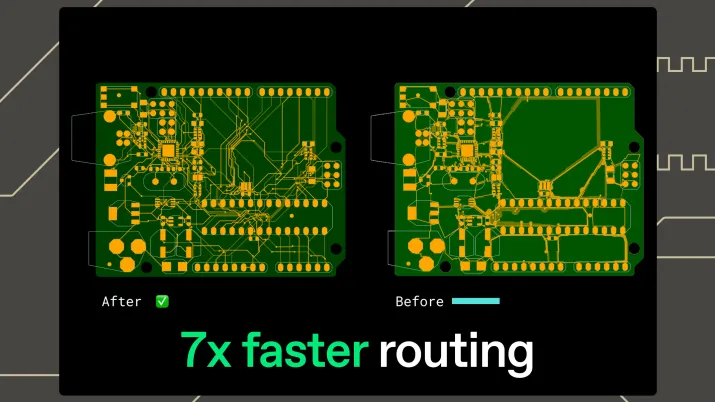
AI駆動型レイアウトツールは、特定の製造業者の能力とファブルールセットを対象とする設計を生成できます。レイアウト生成中に電気的および物理的要件と共にDFM制約を組み込むことにより、これらのツールは最初から製造性に最適化されたボードを生成します。エンジニアは、複数の製造業者を同時に対象とするレイアウトを生成することもできます。実際にルーティングされた設計に基づいて、コスト、リードタイム、および能力トレードオフを比較することができます。