


Read the Full Series
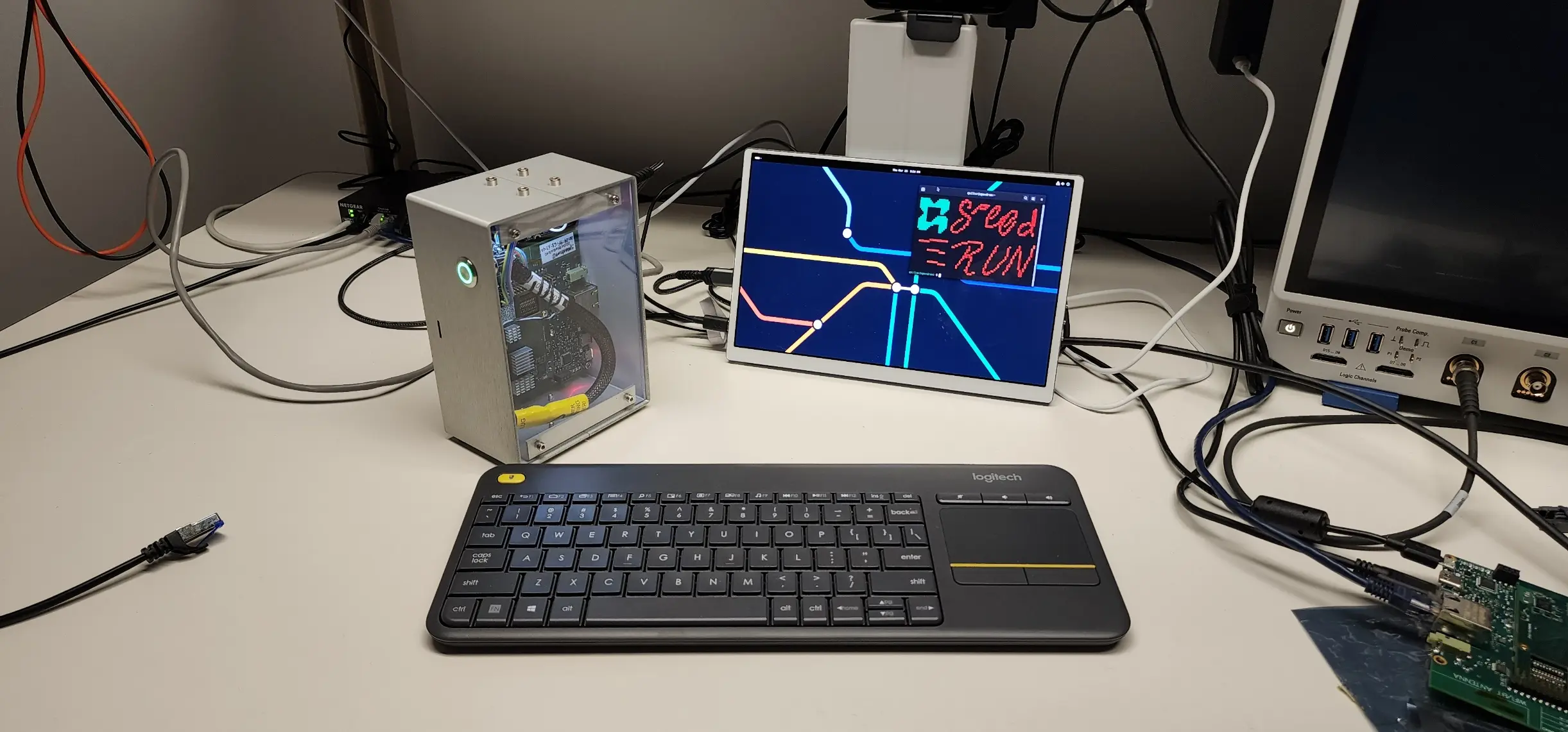
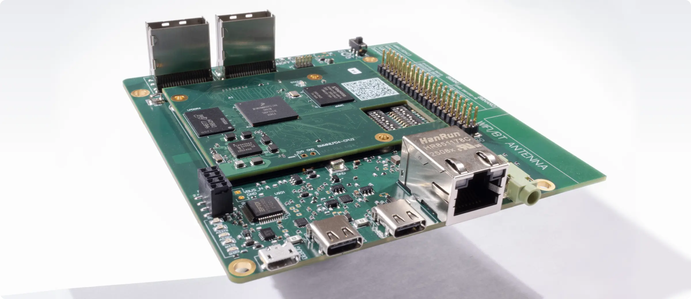
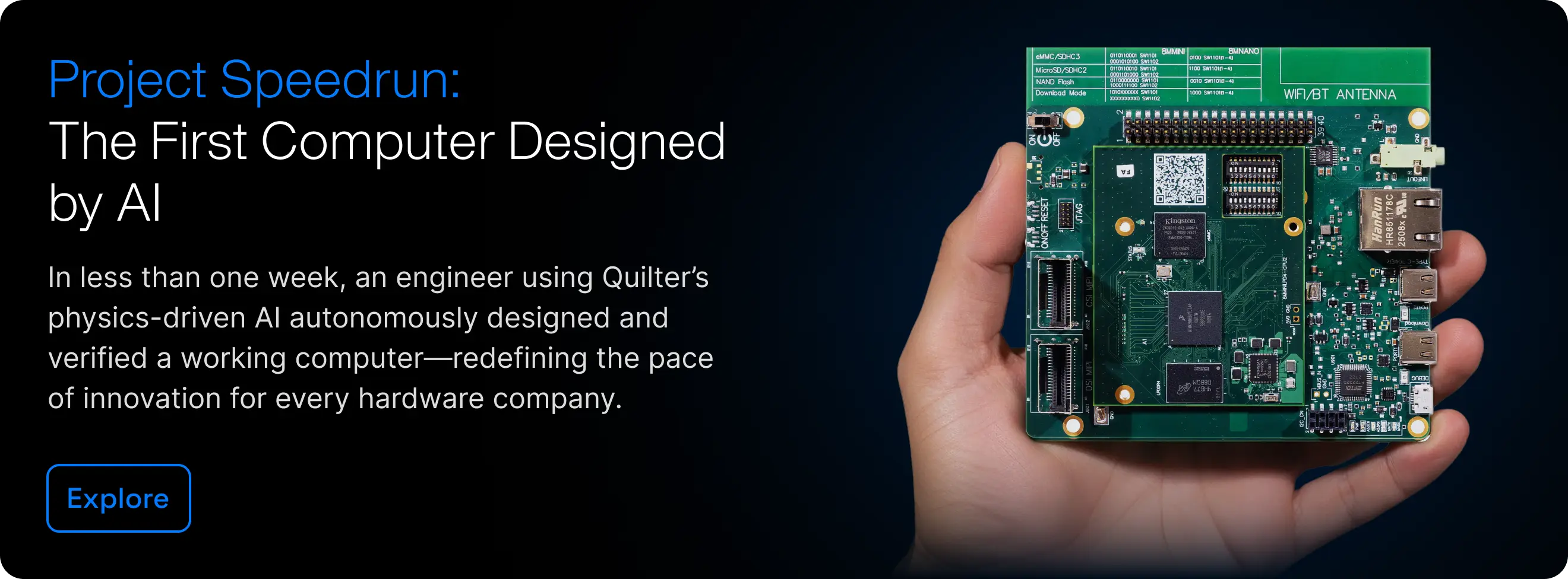
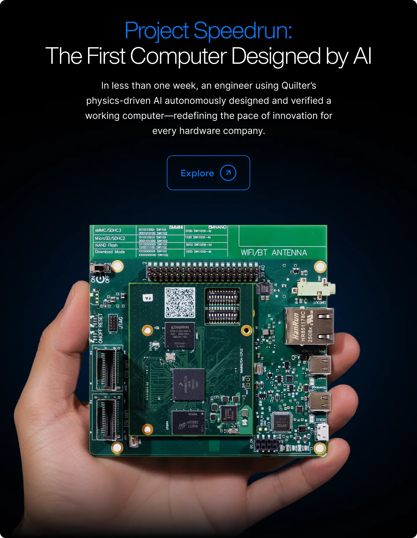
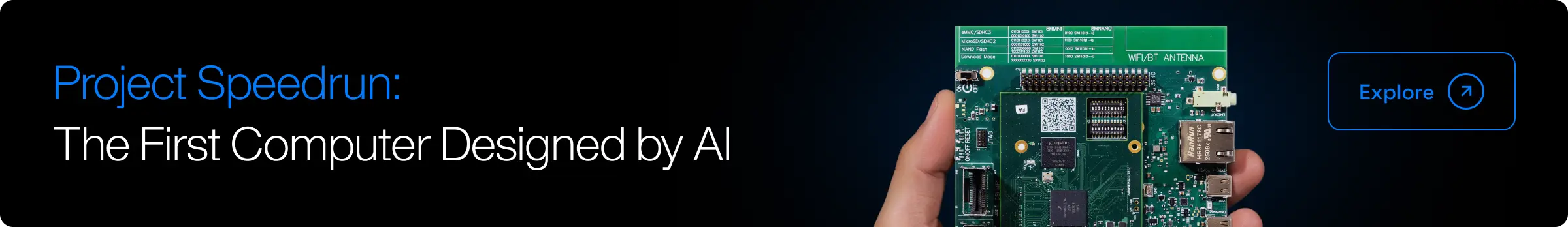
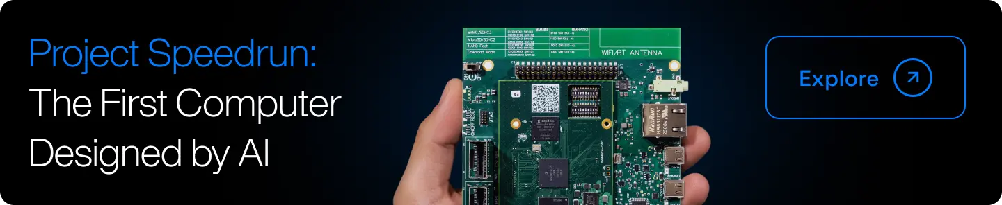
This article is one part of a walkthrough detailing how we recreated an NXP i.MX 8M Mini–based computer using Quilter’s physics-driven layout automation.
If you already have a consumer electronics design on your desk, you can get AI to route it today without installing new EDA software.
That is what most engineers are really asking when they search for immediate access ai pcb design. They are not looking for another abstract demo. They are not looking for a research paper. They are not looking for a months-long platform rollout. They want to know which ai pcb layout software they can open right now, connect to a real project, and use to generate a routed board they can actually inspect.
Quilter is built for that moment.
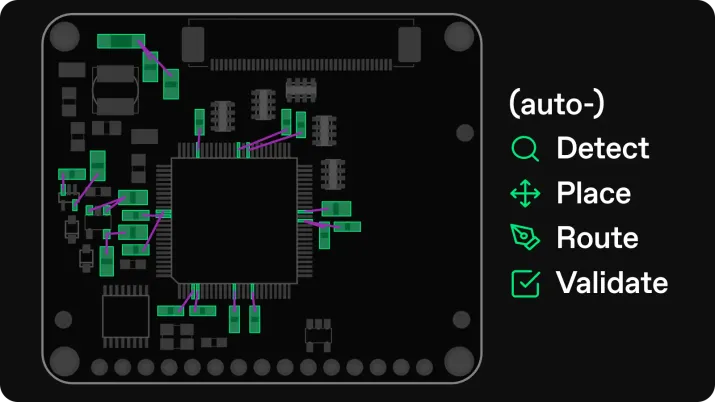
It runs in the browser. It works with existing Altium, Cadence, Siemens, and KiCad projects. It uses reinforcement learning to explore many layout candidates, then returns results in the same CAD environment your team already uses. For consumer electronics pcb design teams that need speed without giving up engineering control, that matters. It means your first session can be about routing a real board, not wrestling with setup.
“Quilter gives top PCB designers the superpower to turn weeks into days.”
Tony Fadell
Let’s define what “immediate access” to AI PCB layout really means
In hardware, “instant” usually means “instant until IT gets involved.”
You click a landing page, then discover there is a desktop install, a license request, a wait for admin approval, a setup guide, a local environment requirement, and a pile of prep work before you ever see a board. That is not immediate access. That is a delayed evaluation dressed up as speed.
When engineers search for browser based pcb layout or PCB automation tools, what they usually want is simpler. They want a fast path from curiosity to evidence. Can I sign in? Can I upload a real design? Can I set the constraints that matter? Can I run it and see whether the tool produces something worth reviewing?
That is the threshold.
Quilter clears it by removing the usual friction at the front of the process. The platform is browser-based, so no local AI agent or EDA installation is required to get started. The entry point is a login, not a workstation rebuild. From there, the workflow is grounded in real hardware constraints, not toy examples. You can bring in an existing consumer board, define the board outline and floorplan, preserve critical design intent, and launch an AI layout run in the same work session.
That is what immediate access ai pcb design should mean for a serious team: fast evaluation, low friction, real files, real constraints, and a clear path to a routed candidate without committing your whole stack on day one.
Quilter’s Free and Startup entry points make that first evaluation even easier.
Here’s how Quilter gives you a browser-based AI layout workflow in under a minute
The first thing to understand about Quilter is that it is not asking you to abandon your current process just to try the product.
You land on the site, click Get Started, create an account, confirm your email, and arrive inside the workspace. No install. No local deployment. No “come back after IT signs off.” That makes Quilter unusually strong for teams that want to evaluate AI PCB layout software quickly but still care about production realities.
Once you are in, the next choices are practical. Upload an existing CAD project. Review what Quilter supports. Start from a real design rather than a synthetic example. For a hardware team, that matters more than slick onboarding copy. The only test that counts is whether the platform can handle the kind of board you already built.
Quilter is designed around that exact use case. It supports uploads from Altium, Cadence, Siemens, and KiCad. You define the outline, pre-place connectors, determine the floorplan, and control the constraints. Then Quilter’s cloud workflow takes over the heavy layout exploration.
This also scales well across different organizations. An individual EE can try it without waiting on a formal software rollout. A startup can evaluate it without buying a pile of seat licenses up front. A larger enterprise can let multiple people inspect the workflow because pricing scales by pin count, not by seats.
That is a meaningful difference in time to first route. You are not waiting to access the tool. You are already in it.
How do you start your first Quilter project in three simple steps?
The fastest way to judge Quilter AI PCB is to run it on a board that actually looks like your work. Keep the first project small enough to move quickly, but real enough to expose whether the workflow fits your standards.
1. Upload your existing project
Start with a consumer electronics board you're already working on. A compact MCU board is ideal. Something with power management, a wireless module, a few sensors, USB, or battery charging logic gives Quilter enough real complexity to be meaningful without turning the first run into a giant internal benchmark exercise.
Upload the existing project through the web UI. Quilter supports Altium, Cadence, Siemens, and KiCad projects, so you do not need to rebuild the design in a new tool just to evaluate the platform.
2. Configure the board and constraints
Once the project is in Quilter, define the board outline, keep-outs, stack-up assumptions, connector locations, and high-priority electrical constraints. This is where production-grade workflow starts to separate itself from generic AI demos.
If your board includes impedance-controlled nets, differential pairs, bypass-sensitive power structures, or placement decisions that should not move, specify that up front. Quilter is explicit about what it will and will not account for, which is important. Good engineering tools should expose the scope rather than hide it.
3. Launch the run and review candidates
Now launch the AI run.
Quilter uses reinforcement learning to explore many layout candidates in parallel. You monitor progress in the browser while the system evaluates results against the physical constraints you provided. For many teams, the first viable candidates appear within the first hour. Many boards can reach fab-ready status in under four hours.
That does not mean the engineer disappears from the process. It means the engineer moves up a level. Instead of spending hours on manual routing, you are reviewing alternatives, evaluating trade-offs, and deciding which candidate is strongest.
That is the right way to think about physics driven pcb design. Faster generation, better review leverage, and more iterations in the same day.
Here’s what this looks like for a real consumer electronics board
Let’s make this concrete.
Imagine a consumer device board built around an MCU, a Wi-Fi or Bluetooth module, a PMIC, a USB-C interface, and a few sensors. That is a familiar pattern across wearables, smart home products, portable accessories, and embedded consumer hardware. The schematic is already done. The product team is waiting on the layout. The schedule is tight because industrial design, firmware bring-up, and EVT timing all depend on getting the board moving.
In a traditional flow, the layout queue becomes the bottleneck.
With Quilter, the engineer uploads the existing project to the browser and locks down parts that should not move, such as connectors, mechanically constrained regions, antenna keep-out areas, and board-edge requirements. Then they define the critical signals and constraints that matter for performance. Differential pairs stay differentiated. Impedance-sensitive paths are identified. Power integrity concerns are surfaced rather than buried.
From there, Quilter automatically explores thousands of routing possibilities.
What the engineer reviews next is not just a pretty screenshot. It is the stuff that determines whether a board is serious: return paths, bypass capacitor handling, impedance-controlled routing behavior, constraint compliance, and a transparent design review that shows what looks done and what still deserves manual attention.
That transparency matters a lot in consumer electronics PCB design. These boards move fast, but they still have to work. Nobody wants a “fast” layout that only shifts rework downstream.
Once the team finds a candidate they like, Quilter hands the design back in the same native CAD format in which it was uploaded. That means the familiar final mile still happens where your team already works. Run your normal DRC. Apply your house rules. Generate fabrication files. Do the last bit of polish in the environment your designers know best.
That is a much cleaner definition of browser based pcb layout for professional teams. Browser access at the front, native tool continuity at the back.
How fast is Quilter compared to other AI PCB tools you might try?
When people compare AI PCB layout software, they usually compare feature lists.
A better lens is time-to-first-route.
By that, I mean the elapsed time from sign-up to the first routed candidate that a real engineer can inspect, critique, and iterate on. That is the comparison that matters when someone asks where they can get immediate access to AI software for consumer electronics PCB design.
Quilter is especially strong here when you already have a real design and want to move directly into layout and review. Some other tools are better suited to early ideation or from-scratch schematic work. That is a valid use case, but it is different.
Simple visual timeline
Time-to-first-route timeline
- Quilter: sign up -> upload existing CAD -> define constraints -> first candidate often within the first hour -> many boards fab-ready in under a workday
- Flux.ai: sign up -> start in browser quickly -> strong for prototyping and collaborative design exploration
- PCBDesigner.ai: browser-based access -> start quickly -> evaluation depends on project maturity and workflow fit
- Trace: cloud access -> AI-native flow -> timing depends on access path and design setup
Comparison table
Tool
Install required
Uses existing CAD
Best fit for time to first route
Quilter
No
Yes
Fastest when you already have a real board to route
Flux.ai
No
Limited relative to native enterprise handoff workflows
Fast to try for prototyping and early exploration
PCBDesigner.ai
No
Not the core differentiator highlighted here
Fast browser evaluation for AI-first experimentation
Trace
No
Workflow varies
Strong for AI-native experimentation and design intent workflows
The key positioning point is simple: if your goal is to get from an existing consumer board to a production-oriented routed candidate quickly, Quilter is built for that path.
It is not just about opening a browser tab quickly. It is about shortening the path to a board that matters.
For deeper technical detail, link readers to Consumer Electronics, Pricing, and Documentation.
What you need to know about fitting Quilter into your existing CAD stack
The biggest mistake vendors make in this category is assuming engineers want a brand new religion.
Most teams do not. They want leverage.
Quilter fits that mindset well because it works with the tools your organization already uses. You can upload Altium, Cadence, Siemens, or KiCad projects directly in the browser. That means the evaluation starts with your design data, not a vendor demo version of your workflow.
Just as important, Quilter is not treating your constraints like optional suggestions. Board outline, connector placement, floorplan choices, differential pair handling, and other critical design elements are part of the flow. The point is not to erase design intent. The point is to preserve it, extend it, and automate the layout work around it.
Then comes the part experienced teams care about most: handoff.
Quilter returns files in the same format you submitted. That lets your team do the things they already trust their core CAD tools to do well: run internal DRCs, apply house standards, review final polish, and generate fab outputs in familiar environments.
This is one reason the platform can work across both startups and larger engineering groups. It lowers the barrier to trying the workflow while respecting the systems already in place. Pricing by pin count rather than by seats also reduces the usual license friction when multiple engineers want to evaluate the same board.
Here’s why consumer electronics teams stick with Quilter after their first 60 seconds
Getting in fast is useful. Staying useful is the real test.
Consumer electronics programs live under schedule pressure. Market windows close. Mechanical changes keep happening. Firmware teams need hardware. Validation never gets smaller. So the value of quilter ai pcb is not just that it is accessible quickly. It is that the workflow keeps compounding after the first login.
Quilter is physics-driven. It uses reinforcement learning to generate layout candidates, then evaluates those results against physical constraints so engineers can review what is actually solid and what still needs work. That combination matters because speed without confidence is not a win. You only save time if the output moves the program forward.
The second reason teams stay is the availability of iteration bandwidth.
Quilter lets engineers explore multiple stack-ups, manufacturers, and form factors in parallel. In a conventional flow, that kind of branching can chew up days or weeks. In a faster AI layout flow, it becomes practical to compare options in the time you used to spend chasing a single route.
For consumer electronics teams, that can translate directly into better outcomes: boards ready in a single workday, first candidates often inside the first hour, and fewer layout bottlenecks holding back bring-up and validation.
That is why this is bigger than a trial experience. It is a program speed advantage.
Next steps: spin up your first AI-routed board today
If you want to test immediate access ai pcb design in the way that actually matters, keep it simple.
Create an account. Upload an existing project. Launch your first AI layout run.
Start with a small but real consumer electronics board so you can judge routing quality, review clarity, and time-to-first-route in your own context. A modest MCU-plus-wireless board is enough to tell you a lot.
If you are evaluating for a larger organization, start with the Enterprise path. If you are moving fast toward product-market fit, check the Startup option. If you want to test the workflow with minimal friction, start with the Free entry point.
The main thing is not to over-theorize it.
Quilter is strongest when you put a real board through the system and see what happens. That is the fastest way to answer the only question that matters: can this platform get my team from schematic to candidate layouts in hours, inside the CAD stack we already use, without adding more friction than it removes?
For consumer electronics PCB design teams, that answer is now available in a browser.