PCB Fabrication
What Is PCB Fabrication?
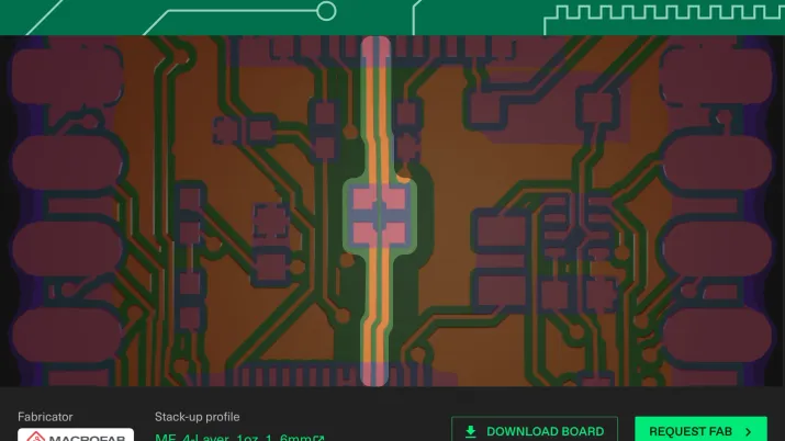
PCB fabrication is the manufacturing process that transforms raw materials — copper-clad laminate, prepreg, solder mask, and silkscreen inks — into a finished bare circuit board ready for component assembly. The process involves multiple steps: inner layer imaging and etching, layer alignment and lamination, drilling of through-holes and vias, copper plating, outer layer imaging and etching, solder mask application, surface finish application, silkscreen printing, electrical testing, and final profiling to the board outline dimensions.
Each fabrication step has associated capabilities and limitations that the PCB designer must account for during layout. Minimum trace widths and spacings, smallest drill sizes, annular ring requirements, aspect ratios for plated holes, solder mask registration tolerance, and layer-to-layer alignment accuracy all vary between fabrication facilities and technology levels. Designing within these capabilities ensures that the board can be manufactured reliably and cost-effectively; pushing beyond them results in lower yields, higher costs, and longer lead times.
Fabrication-Ready Outputs From AI Layout
One of the core value propositions of physics-driven AI layout tools is producing designs that are fabrication-ready by construction. By incorporating the target manufacturer's design rules and capabilities as hard constraints during layout generation, the AI engine ensures that every trace, via, pad, and clearance in the generated design falls within the fabricator's proven process window. This dramatically reduces the number of DFM review iterations between the design team and the fabrication house, shortening the time from design completion to board delivery.