Controlled Impedance PCB
What Is a Controlled Impedance PCB?
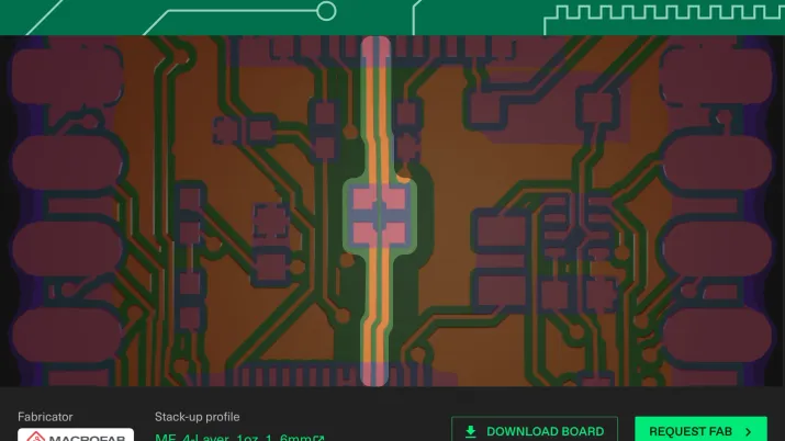
A controlled impedance PCB is a printed circuit board that has been designed and manufactured to achieve specific characteristic impedance values on designated traces. Unlike standard PCBs where trace width is chosen primarily for current capacity and routing density, controlled impedance boards specify trace widths calculated to achieve target impedance values (such as 50Ω single-ended or 100Ω differential) based on the stackup dimensions and dielectric properties. The fabricator manufactures test coupons alongside the production boards and measures the actual impedance using a Time Domain Reflectometer (TDR) to verify compliance with the specified tolerance, typically ±10%.
Controlled impedance is mandatory for any PCB carrying high-speed digital signals where transmission line effects are significant. This includes virtually all modern computing, networking, and communication interfaces: PCIe, DDR, USB 3.x and above, HDMI, Ethernet above 100 Mbps, SATA, and high-speed serial protocols. The impedance specification flows from the interface standard through the stackup design to the fabrication process, creating a chain of precision that must be maintained at every step to ensure reliable signal transmission.
End-to-End Impedance Management
Controlled impedance design requires tight coordination between the layout engineer, the stackup designer, and the fabrication house. Physics-driven AI layout tools can manage this coordination internally by computing trace widths from the stackup geometry and material properties, verifying that impedance targets are met across every layer and routing path, and generating fabrication notes that communicate impedance requirements clearly to the manufacturer. This end-to-end impedance management eliminates the manual handoffs and spreadsheet calculations that traditionally introduce errors into the impedance specification chain.