Blind Via
What Is a Blind Via?
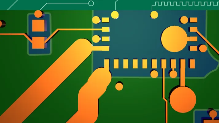
A blind via is a plated hole in a PCB that connects an outer layer (top or bottom) to one or more inner layers without passing through the entire board stackup. Unlike through-hole vias that span all layers, blind vias are drilled from one surface and terminate at an internal layer, making them invisible from the opposite side of the board. This selective layer connectivity allows designers to use board real estate more efficiently, particularly under dense BGA packages where routing space is at a premium.
Blind vias are manufactured by drilling and plating individual layer pairs before the full stackup is laminated together, which adds complexity and cost to the fabrication process. The aspect ratio (depth-to-diameter ratio) of blind vias must be carefully controlled — most fabricators limit blind via aspect ratios to 1:1 or less to ensure reliable plating quality. Designers must balance the routing density advantages of blind vias against the increased manufacturing cost and longer lead times they introduce.
Optimizing Via Types in AI-Generated Layouts
Choosing between through-hole vias, blind vias, buried vias, and microvias is one of the most impactful decisions in PCB layout — affecting routing density, signal integrity, manufacturing cost, and lead time. Physics-driven AI layout engines can evaluate multiple via strategies simultaneously, generating design candidates that use different via combinations and allowing engineers to compare the tradeoffs in routing completion, layer utilization, and manufacturability. This parallel exploration replaces the traditional approach of committing to a via strategy upfront and hoping it proves sufficient during routing.