


Blind and Buried Vias
Support for blind and buried vias is in active development. Today Quilter routes through-vias only. This work unlocks HDI boards and other dense modern designs that depend on multi-tier via structures.
Quilter is improving with every release. This page tracks what's new, what changed, and what we're working on next.


May 31, 2026
Copy link
Support for blind and buried vias is in active development. Today Quilter routes through-vias only. This work unlocks HDI boards and other dense modern designs that depend on multi-tier via structures.
Read more
May 1, 2026
Copy link
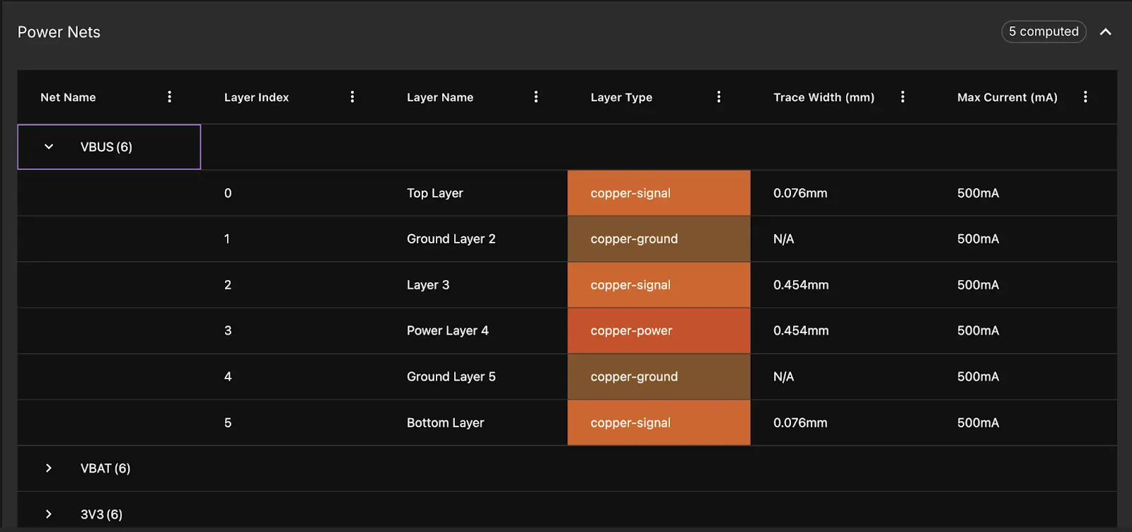
Quilter now reads net-class clearance rules, layer-specific clearances, and pair-specific clearances directly from your input files and respects them throughout placement and routing. This is the foundation for stronger DRC checks and higher-fidelity output. In the early beta version it happens silently, and there is a UI display of the detected constraints coming soon. Support for other ECADs is also under development.
How it works: This is now the automatic behavior for Altium files, though you won’t see a review in the UI.
Coverage: Altium Constraint Manager only, with other ECADs in the coming months.
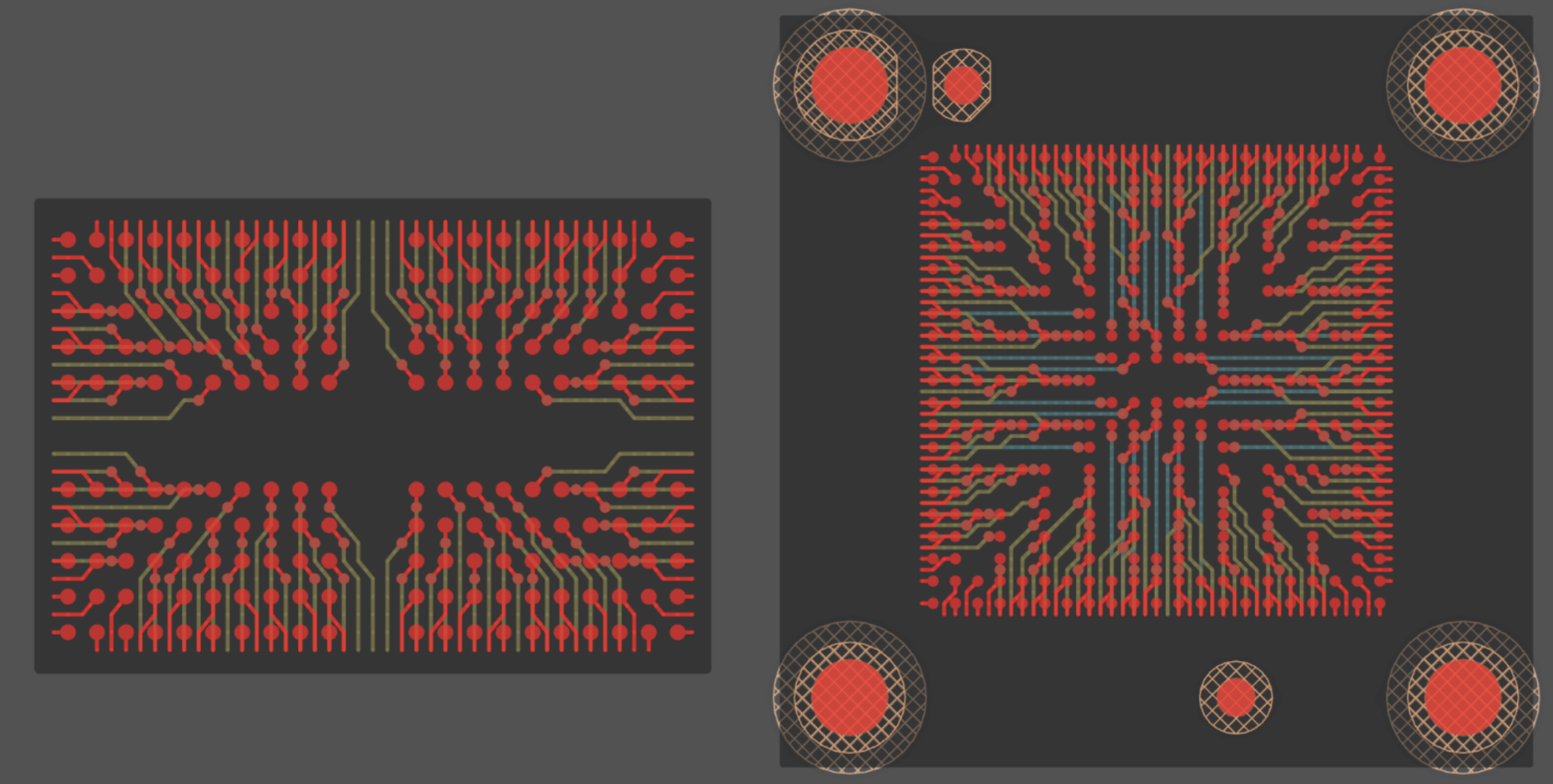
Quilter now generates fanout and breakout for BGAs automatically as part of standard candidate generation. BGAs no longer need to be pre-fanned-out in your ECAD tool before submission.
How it works: Choose “Generate Fanout” in the BGA Component section of the Comprehensions page, and Quilter will select via patterns, escape directions, and breakout routing for each BGA on the board based on the stackup.
Coverage: BGAs with square ball patterns common on application processors and high-density connectors.
Why this matters: BGA fanout has been one of the most common parts of manual prep work customers did before submitting a board. Removing that step shortens setup and improves routing quality on dense designs, because Quilter is no longer routing around a fanout it didn't choose.
You can now override Quilter's computed impedance constraints directly in the app. This makes it quick to use your own impedance values or update ours without going back to your ECAD tool to make changes.
This pairs with the calculated impedance profiles released in April. The default behavior is still to compute impedance from your stackup using Simbeor, but when you need a different value for a specific net, you can set it inside the job setup flow.
Docs: Single-ended Impedance Control, Differential Pairs
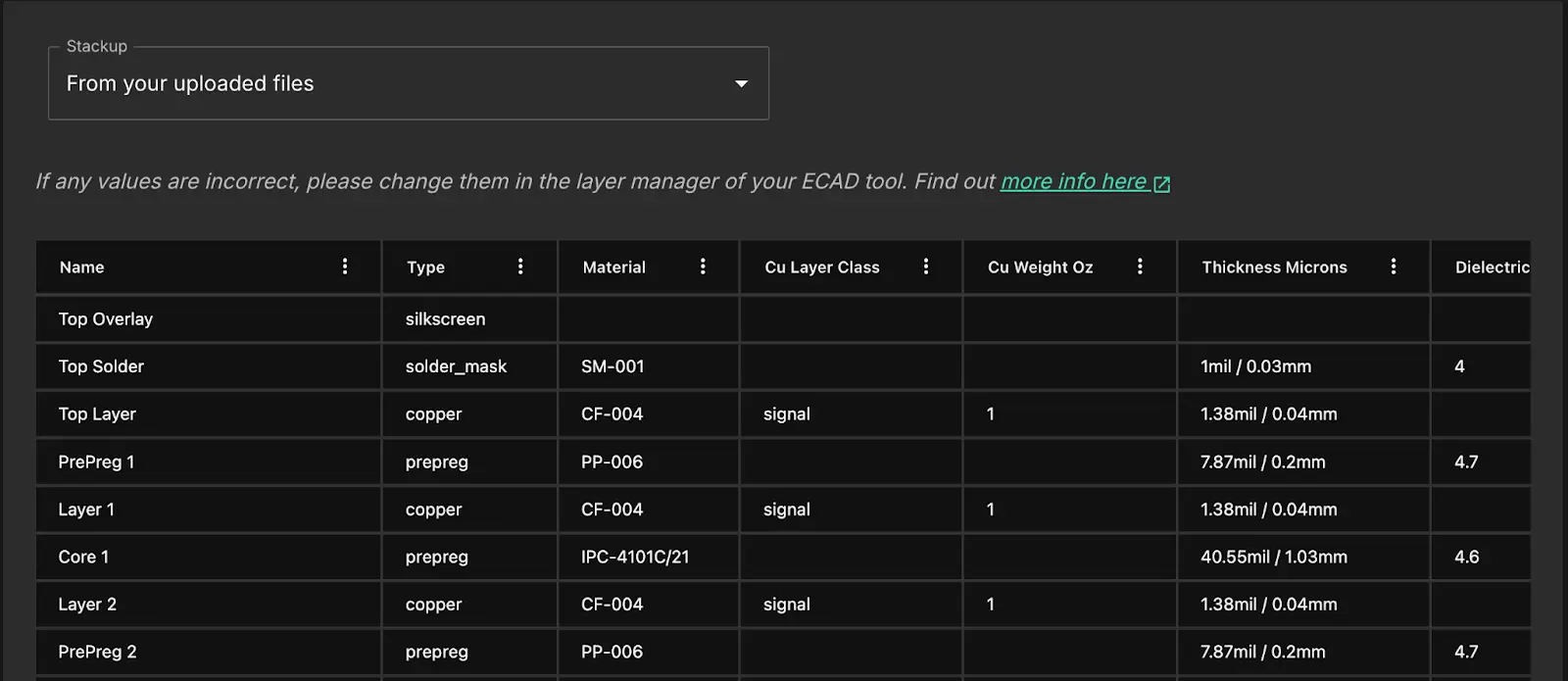
The job setup flow now surfaces stackup and fabricator constraints more explicitly. Each layer, material property, and fabrication rule that affects routing is visible in the setup screens, and the fab constraints are editable within the app. In the next week or two, layer assignments will also be editable. This continues the work started by the restructured setup flow in March: fewer parameters that get applied silently, more parameters you can see and adjust.
Docs: Stack-ups, Specify design parameters
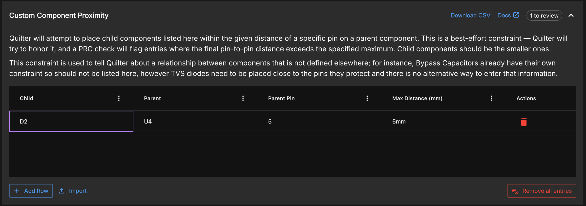
A new constraint type for specifying that one component must sit close to a specific pin on another component. Available in Step 5.2 of the app under "Define your own constraints."
How it works: Select the restricted component, the parent component, the target pin on the parent, and the maximum allowed distance. Quilter applies the constraint during placement and verifies it in the physics rule check, the same way it handles every other placement constraint.
Why this matters: Some constraints (a current sense resistor next to a specific pin on a power IC, a snubber close to a specific FET pin) couldn't be expressed cleanly before. Customers either pre-placed those components themselves or routed the intent through the bypass cap flow. This adds a direct way to express component-to-pin proximity.
Related docs: Physics Constraints Overview, Placement regions
Read more
April 7, 2026
Copy link
Quilter can now calculate impedance profiles for differential pairs and single-ended impedance-controlled signals across all layers of your board, based on your stackup materials. Give Quilter any stackup on any board, and it will route using the trace widths and clearances needed to hit your target impedance.
The calculations are powered by Simbeor by Simberian, the industry-standard solver. If you’ve used impedance calculations in Altium, you’ve already used this solver. As long as the material properties in your stackup are correct, the impedance profiles will be correct.
Jobs now belong to projects. A project groups every iteration of a single design (different board outlines, stackups, floor plans) into one place, so you can track your progress and pick up where you left off.

How it works: Create a new project from the home screen and upload your first job. From there, you can add as many jobs as you need, as long as each upload stays within 10% of the original BOM. Changes beyond 10% start a new project.
Why this matters: Most Quilter customers iterate 2 to 4 times on a design before going to fab. Projects make that workflow explicit: one design, unlimited iteration, everything in one place. This structure also lays the groundwork for faster solve times on subsequent iterations within the same project.
Previously submitted jobs are still accessible from your jobs list. Going forward, all new jobs require a project.
See the Project Documentation for setup details.
Read more
March 26, 2026
Copy link
This release makes Quilter more explicit about how it interprets your board. New ground net comprehension and a restructured setup flow that surfaces constraints you may otherwise have missed. Single compile target ensures that you get the stackup and constraints you intended.
You can now explicitly choose which ground net Quilter uses on your ground layers. Previously, Quilter made a calculated guess at the primary ground. That worked in most cases, but was a fallible assumption on boards with multiple ground domains.
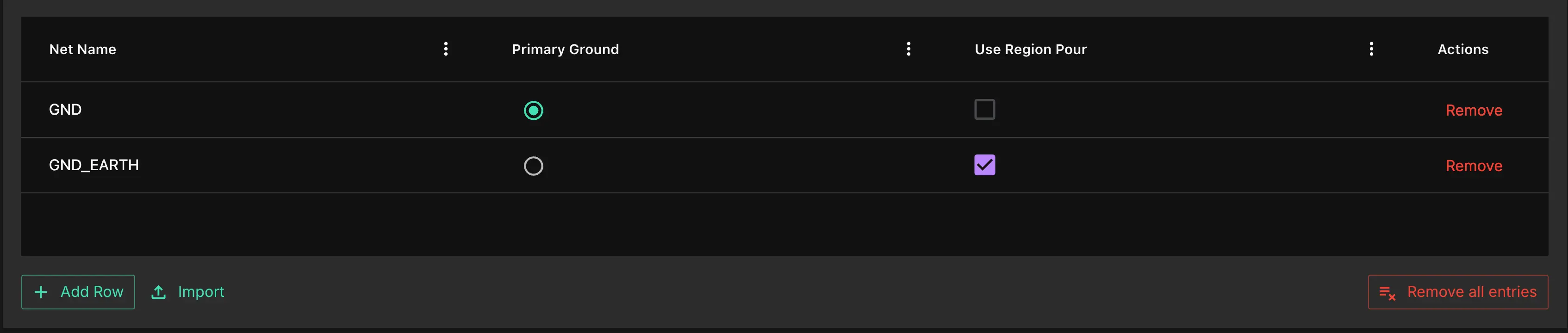
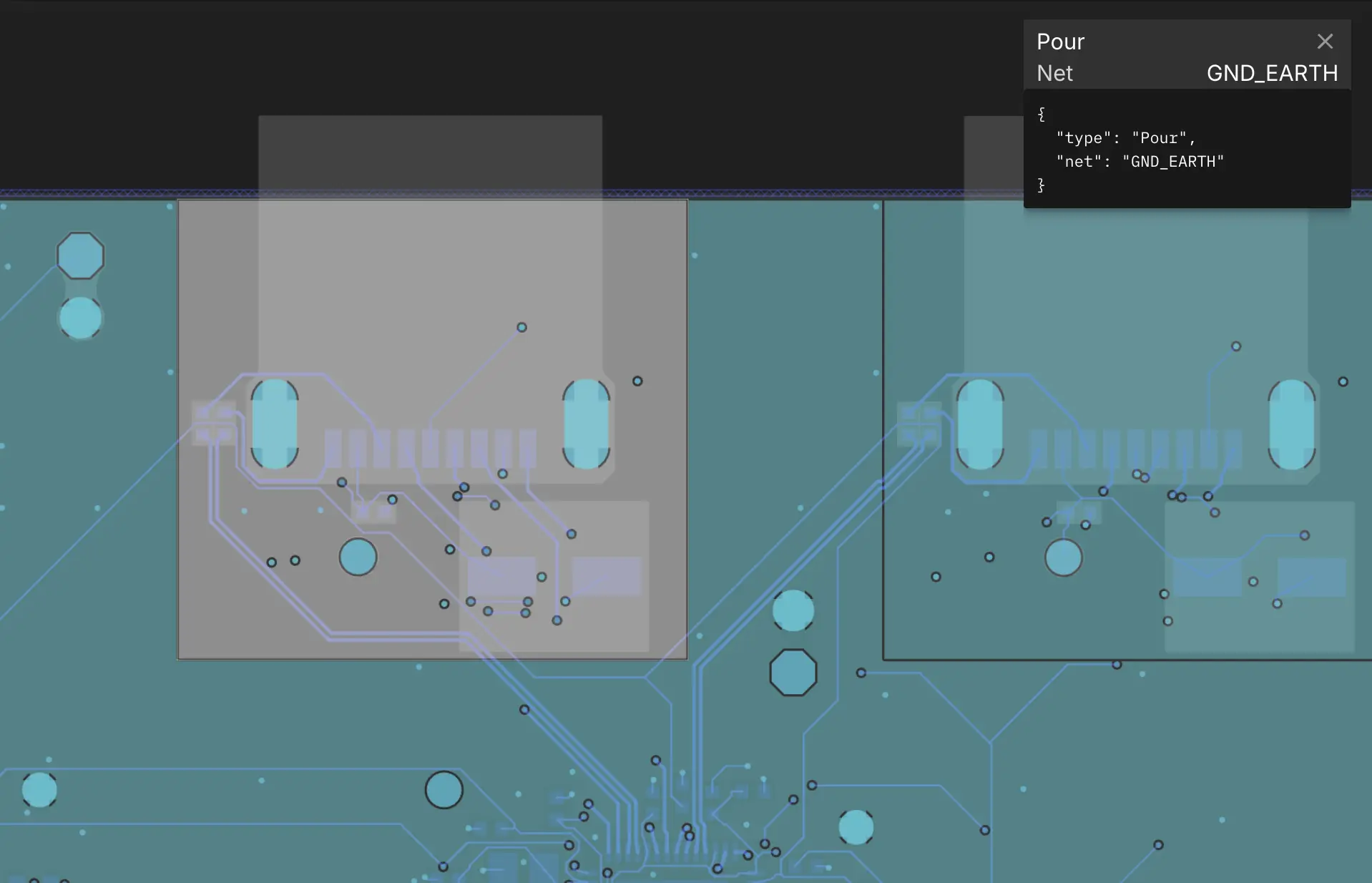
This update also enables region ground pours. If you have a placement region where components share one ground net, Quilter can now establish an independent ground plane for that region. This is directly useful for isolation, high-voltage sections, and sensitive signal domains.
The job setup flow has been restructured from two pages into four, with significantly more detail at each step. The new flow explicitly surfaces your stackup layers, power and ground assignments, and fabricator constraints. It also shows which specific constraints Quilter has calculated from your inputs, like what net width will be used to meet IPC2221 heating requirements on each layer for a high power net with a known current.
The goal: reduce the chance that something gets misconfigured silently. Every parameter that affects routing quality is now visible and editable before you submit.
Until now Quilter has attempted many stackups and design constraints within each job. This can be useful for exploring possible solutions, but most of the time you know what parameters are required. Including the many stackups made it more awkward to define as single one clearly, and this change supports the improvements listed above in Restructured Setup Flow. Now you’ll have better control and clarity of how Quilter will construct your board.
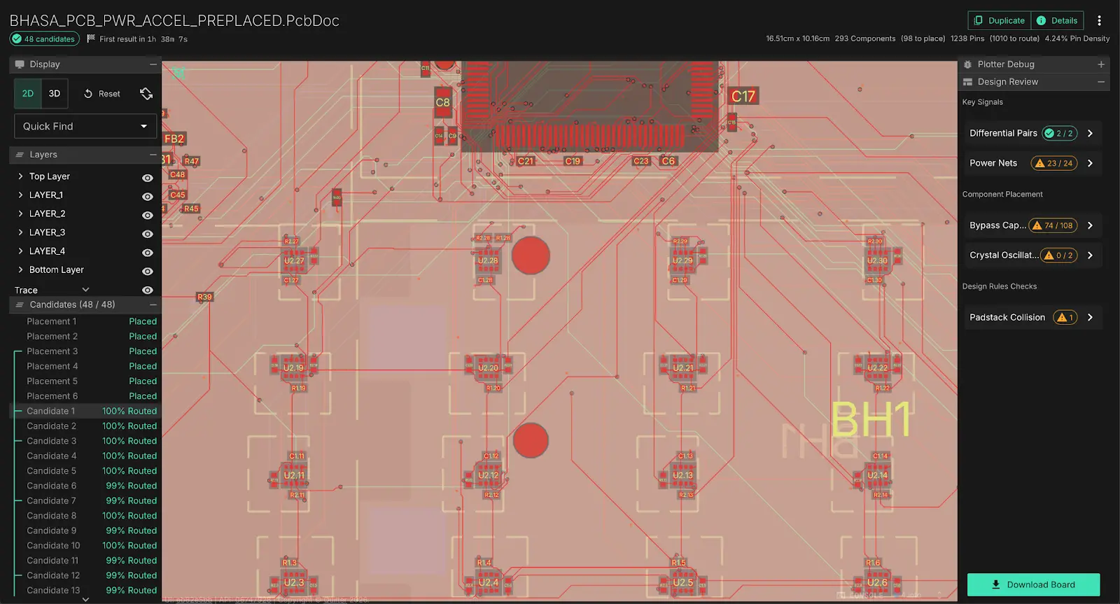
Looking at your routed boards is even easier with the new full screen redesign. The “Detail View” mode has consumed all the panels and become the default, so now it’s easy to see everything at once without switching around. The redesign also works well on large monitors.
Read more
December 31, 2025
Copy link
Specifically: preserving the intent you already expressed in your ECAD tool and carrying it all the way through placement and routing without forcing you to over-configure or babysit the process.
We shipped four pillar updates last year: power pour generation, regions and smart clustering, stackup import, and keepout updates. Together, these changes reduce ambiguity in how the system interprets your board and materially improve routing quality, EMI behavior, and predictability.
Power pours—large copper quilter-filled areas tied to a specific power net — provide a low-impedance path for current, reducing voltage drop and heat, but have historically been a tedious, manual process in traditional CAD tools.
Quilter handles the entire workflow automatically: it detects likely power nets by name, prompts you to select which ones to pour, optimizes component placement to improve pour continuity, generates filled copper regions that respect spacing and keep-out rules, and runs physics rule checks on trace width and current capacity—all as part of standard candidate generation with no extra manual steps.
You can now define placement regions directly in your ECAD tool and have them respected on import. Regions act as geometric constraints for placement, collecting components that must stay together, stay local, or stay isolated. Regions can be single-sided or two-sided, which is particularly important for dense designs and mixed-signal boards where vertical separation is just as intentional as horizontal grouping.
Quilter has also introduced smart clustering, where components that are directly connected within a schematic are placed close together.
Another new feature is “anchoring”, which allows you to place a single component from a cluster and have all the other components from the cluster snap to it, saving you time in manual placement.
See the Placement Guide to learn more!
On import, Quilter reads stackup and design requirements directly from your input files. That means: layer order is preserved, dielectric context is known, design rules are reflected in minimum trace width, via size, etc
Keepouts are now first-class constraints and support any combination of traces, vias, components, and pours. You can define keepout regions in your ECAD tool to: protect antennas, reserve mechanical space, block routing under sensitive ICs, and respect your component internal areas.
On import, Quilter respects these regions and enforces them during placement and routing.
This is a high-visibility, high-value feature because it prevents entire classes of late-stage failures like EMI problems, RF degradation, and undesirable placement before they start. Behind the scenes, this work lays the foundation for broader design rule ingestion, including full clearance constraint support and stronger DRC checks coming soon.
Read more
