


Read the Full Series
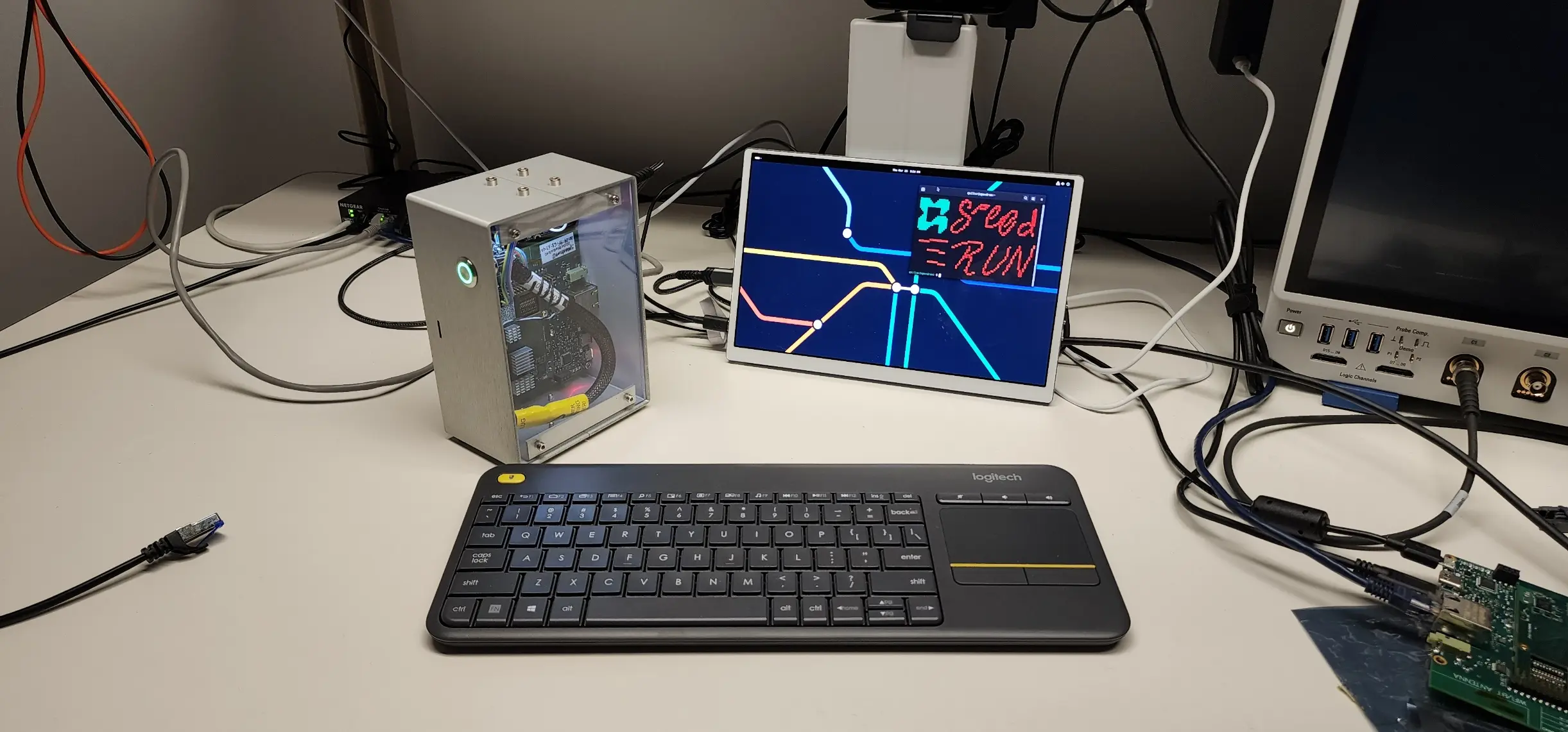
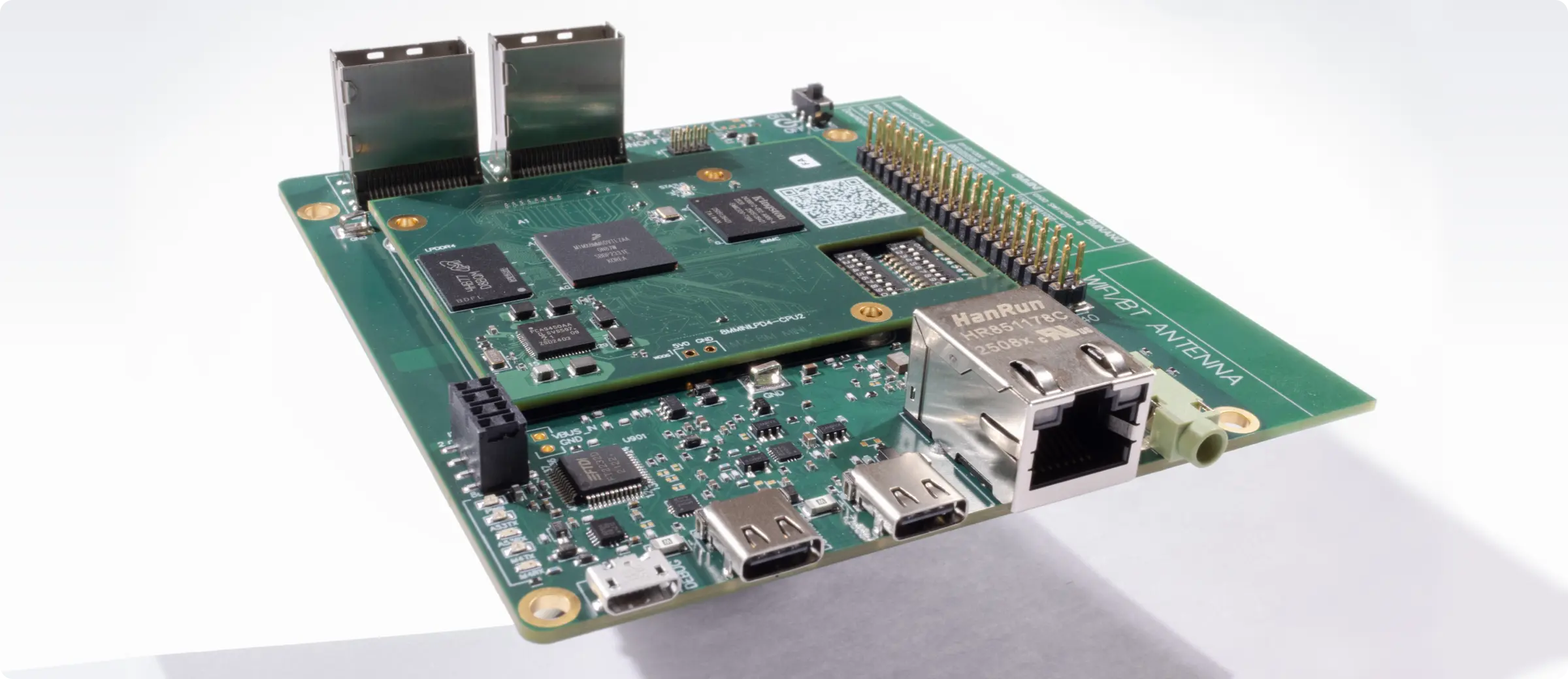
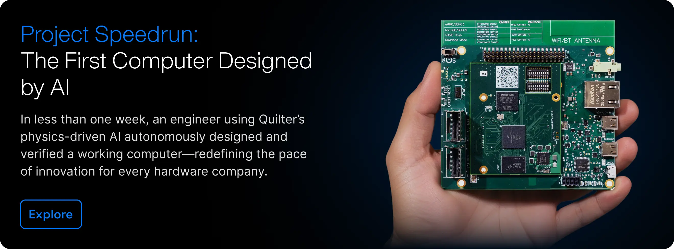
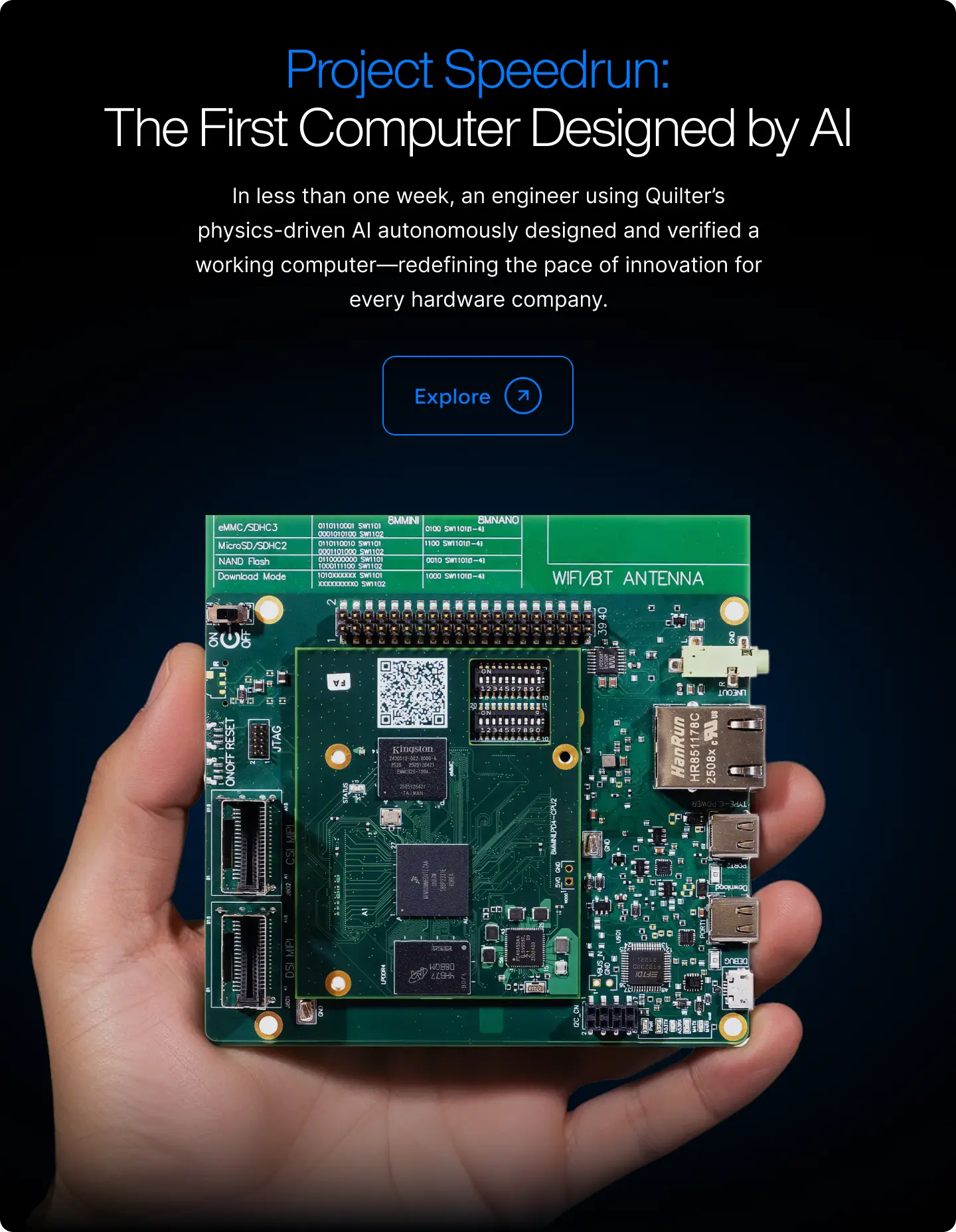
This article is one part of a walkthrough detailing how we recreated an NXP i.MX 8M Mini–based computer using Quilter’s physics-driven layout automation.
If you design PCBs on Linux, you already know the tradeoffs. You want stability, performance, and real control over your environment, but you also want tools that keep pace with modern hardware design. The challenge is simple: many legacy EDA tools were built for Windows first, and Linux users have spent years navigating package issues, compatibility fixes, and workarounds. The good news is that Linux-native EDA options have grown stronger, and cloud-native platforms are creating a new path forward.
This guide gives you a complete comparison of Linux-friendly PCB design software. We will break down native applications, emulated Windows tools, and a new class of cloud-based design platforms. Then we will show where Quilter fits in for engineers who want top-speed layout and zero setup friction on Linux.
Let's define what matters most for Linux PCB designers
Choosing PCB design software on Linux is not the same as choosing software on Windows or macOS. Linux engineers care about reliability, automation, reproducibility, and control. That creates a different set of expectations for EDA tools.
Linux is the natural home for many hardware engineers
Linux offers package managers, scripting flexibility, and stable development environments that fit perfectly with hardware workflows. Engineers who prefer open standards, deterministic tooling, and minimal vendor lock-in tend to gravitate toward Linux.
Common frustrations with traditional EDA tools
Many legacy PCB tools depend on Windows-only installers, proprietary drivers, or desktop environments that do not translate cleanly to Linux. Even when they run through Wine or a VM, engineers must deal with quirks like limited GPU acceleration, slow rendering, unstable hotkeys, and file-system problems.
Why native and open standards matter
Linux users tend to prioritize:
- Native applications that integrate cleanly with package managers
- Well-documented file formats
- Stable long-term compatibility
- No dependency chains that break during updates
- Workflows that support scripting, automation, and open collaboration
These needs shape the selection of the best PCB design software for Linux. Native tools get you part of the way there. Cloud-native tools take the rest of the burden off your system entirely.
How do the top native Linux tools stack up?
Native Linux PCB tools have improved significantly in the past decade. The leading options are KiCad, LibrePCB, gEDA/PCB, and pcb-rnd. Each one targets slightly different users, workflows, and design complexity levels.
Below is a clear, practical comparison so you can decide which fits your environment.
Native Linux PCB Tools Comparison Table
Real-world scenarios
Scenario 1: I am a hobbyist working on small 2 to 4 layer boards
KiCad or LibrePCB are the top picks. LibrePCB wins on simplicity. KiCad wins on depth and long-term growth.
Scenario 2: I am a startup engineer building 6 layer or 8 layer prototypes
KiCad is the realistic native Linux option, because the others are not optimized for advanced constraints.
Scenario 3: I need extreme scripting and automation
pcb-rnd is the most flexible. Its audience is smaller, but its automation capabilities are strong.
Verdict on native Linux tools
If you want stability, open-source tooling, and clean package installation, KiCad is the safest long-term choice. It scales well as your designs get more complex. LibrePCB is the easiest for new users. The others are strong within niche or legacy workflows.
But native tools still require local installs, dependency management, and manual updates. That becomes more painful when teams grow, especially when not everyone uses Linux.
What challenges come with running Windows PCB tools on Linux?
Many engineers attempt to run Windows-only EDA tools on Linux using Wine, Proton, or virtual machines. While it is technically possible, this path always introduces friction. For production work, that friction compounds over time.
The technical hurdles
Running Altium, OrCAD, or DipTrace on Linux usually comes with obstacles like:
- Slow or inconsistent GPU acceleration
- Limited support for high DPI displays
- Hotkeys or UI interactions that break inside Wine
- Driver or USB passthrough issues when programming MCUs
- File system inconsistencies when saving large project folders
These problems are not catastrophic but add daily friction that slows engineering cycles.
Licensing and update issues
Some Windows EDA tools use licensing systems tied to Windows services that do not always run correctly under Wine. Updates may fail. Support teams may decline to help. This creates additional risk for engineering teams that rely on predictable workflows.
When emulation is viable
Using Windows PCB tools on Linux can work when:
- Your team standardizes on a Windows tool
- You only need occasional access to the tool
- You have a managed VM environment
- You accept the performance hit for the sake of compatibility
This approach is not ideal if you want a native-feeling experience, fast layout iteration, or a fully Linux-first development workflow.
Here's why cloud-native PCB design is changing the game
Cloud-native PCB software removes the entire dependency stack from your local machine. You do not need Wine, VMs, or custom installs. Everything runs in the browser. This is ideal for Linux engineers who want speed, portability, and predictability.
No dependency headaches
Cloud-native tools eliminate the package management and compatibility issues that plague desktop installations. You can use any modern browser and get a consistent experience across distributions.
Seamless cross-OS collaboration
Teams often include Windows and macOS users. With browser-based PCB design:
- Everyone sees the same interface
- No one fights version mismatches
- Files, constraints, and design rules stay consistent
This removes the fragmentation that slows multi-platform engineering teams.
Always up to date
You get:
- Automatic updates
- Automatic security patches
- No local installation or upgrade work
- Instant access to new features
This allows Linux engineers to spend more time designing and less time maintaining tools.
Unlocking new workflows
Cloud-native architecture gives hardware teams new capabilities:
- Parallel layout generation
- Remote reviews
- Cloud-based constraint management
- Shared design candidates
- Unified version control
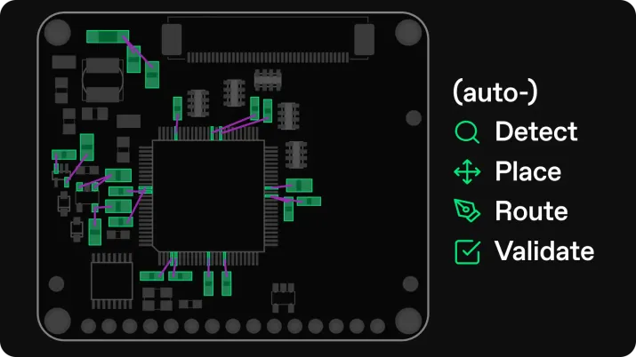
This is where modern AI-driven PCB tools begin to shine.
How does Quilter compare for Linux users?
Quilter is a cloud-native platform designed to accelerate PCB layout using physics-driven AI. Because it runs entirely in the browser, it is instantly compatible with Linux without any installs or system configuration.
Below is a direct comparison of Quilter versus the most common native and emulated options.
Quilter vs Native and Emulated Tools
Why Quilter aligns with Linux priorities
Linux engineers value control, repeatability, and speed. Quilter delivers those by removing local dependencies, reducing manual layout work, and giving teams a browser-based environment that behaves the same everywhere.
Key benefits:
- Zero local installation
- No dependency chains
- Works on any Linux distribution
- AI layout that shrinks design cycles
- Easy collaboration with Windows or macOS teammates
- Full physics-aware validation before handoff
For engineers who want to move fast without giving up complexity or control, Quilter becomes a compelling alternative to both native and emulated tools.
What results can you expect if you switch?
Switching to cloud-native, AI-powered PCB design changes both the pace and quality of hardware development. Linux users tend to see the largest gains because they remove the overhead of managing local CAD configurations.
Faster iteration
You can generate new PCB layout candidates in hours. You can evaluate multiple stackups, routing strategies, and physical constraints in parallel. This increases the number of design cycles your team can complete in the same amount of time.
Higher board quality and reliability
Physics-aware validation catches issues like:
- Impedance mismatches
- Missing bypass capacitors
- Differential pair issues
- High frequency routing errors
The result is fewer surprises during bring-up and less rework.
More productive engineering teams
With layout automated, engineers can focus on:
- System architecture
- High speed interfaces
- Power integrity
- Verification and testing
Teams ship hardware faster and with fewer delays.
If you work in startups, robotics, aerospace, or semiconductor validation, these gains translate directly into shorter R&D cycles and a more predictable development pipeline.
Ready to try modern PCB design on Linux?
If you want a faster, more reliable way to design PCBs on Linux, you can try Quilter for free. No installation. No configuration. Just open your browser, upload your KiCad, Altium, Cadence, or Siemens files, and start generating layouts.
- Sign up here: https://www.quilter.ai
- Visit the documentation: https://docs.quilter.ai
- Join the community: https://community.quilter.ai
- Access Linux-specific support: https://help.quilter.ai
We want to hear from Linux engineers. If you have feedback or feature requests, the Quilter team would love to learn how we can make Linux-based PCB development even better.
Modern PCB design is no longer tied to a desktop install. With cloud-native tools and physics-driven AI, Linux users can design faster, collaborate easier, and build more ambitious hardware than ever.