


Read the Full Series
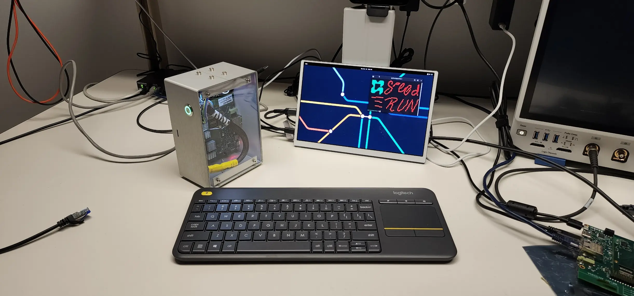
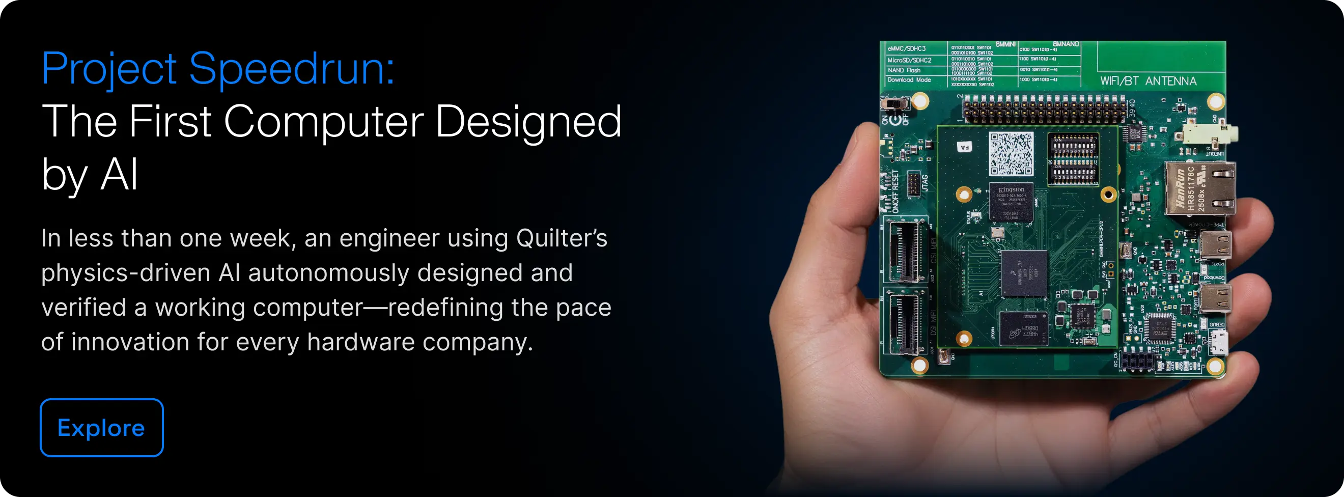
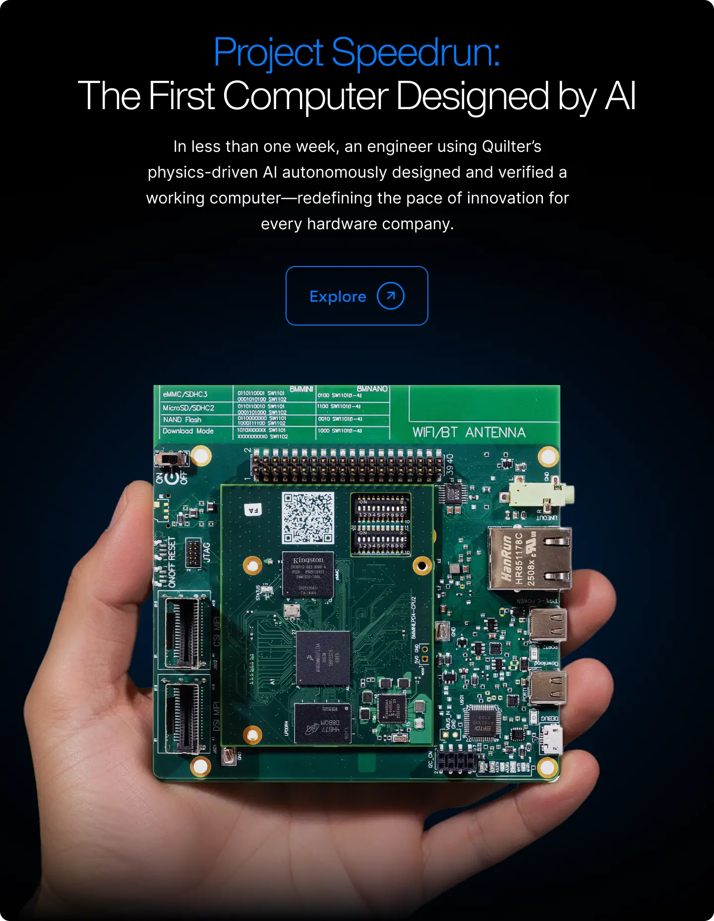
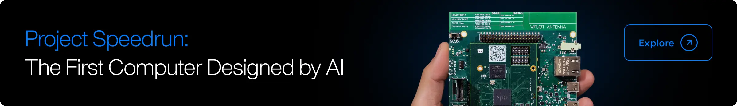
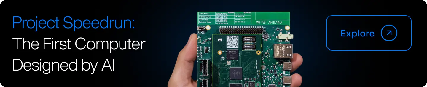
This article is one part of a walkthrough detailing how we recreated an NXP i.MX 8M Mini–based computer using Quilter’s physics-driven layout automation.
Weeks lost to manual layout bottlenecks. Engineers juggling too many tools. Review cycles dragging on because layout cannot keep up with schematic changes. If any of this sounds familiar, your team is probably evaluating new EDA software or wondering if an AI-driven platform could finally break the bottleneck.
Choosing EDA software used to mean picking between a handful of familiar names and hoping the workflow matched your needs. Today the landscape looks very different. AI is automating PCB layout, accelerating iteration, and making physics validation faster and more reliable. For hardware teams trying to move quickly, the decision is no longer about which tool has the nicest UI. It is about which platform helps you design more, learn faster, and hit deadlines with confidence.
In this guide, you will get a clear, practical framework for evaluating EDA tools in a world where AI-first platforms like Quilter are reshaping what teams can expect from PCB design.
This is your definitive guide on how to choose EDA software in the age of AI.
Let's define what EDA software actually does
Before comparing tools or deciding whether AI should influence your choice, it helps to establish what EDA software is designed to do and why each component matters to a modern hardware program.
Electronic Design Automation (EDA) software is the core environment where electrical engineers design and validate the electronic systems that power everything from consumer devices to aerospace systems. At its heart, EDA software provides three essential functions.
First, EDA tools enable schematic capture and circuit design. This is where engineers define components, connectivity, and electrical behavior. A great schematic tool makes it easy to organize symbols, manage libraries, define nets, and spot errors early.
Second, EDA platforms manage PCB layout and routing. This involves placing components, running traces, setting rules for spacing, and creating the physical board that a manufacturer will build. Layout is time consuming and highly constrained. It often represents the largest bottleneck in the hardware development cycle.
Third, EDA software supports simulation, validation, and manufacturability checks. This includes signal integrity analysis, power integrity reviews, design rule checking, and 3D mechanical verification. These checks ensure the final board works as intended when it leaves the CAD environment and enters the real world.
Every EDA tool approaches these functions differently. Some emphasize usability. Some emphasize ecosystem depth. Some emphasize simulation power. Emerging AI platforms emphasize automation and iteration speed. Understanding these foundations helps you make a smarter, more confident decision.
What should you look for before picking a tool?
Choosing EDA software starts with evaluating your team and your projects. Before comparing brands, answer these questions or walk through this checklist. It will ground your decision in your actual workflow rather than marketing claims.
1. How complex are your designs?
- Are you building simple microcontroller boards or high-speed, high-layer systems?
- Do you require controlled impedance, differential pairs, blind and buried vias, rigid-flex, or complex stackups?
- Does your team often redesign boards late in the process due to system changes?
More complexity means greater value from powerful automation, strong simulation features, and consistent rule enforcement.
2. What simulation and analysis capabilities do you need?
- Do you require signal integrity or power integrity analysis?
- Do you work with RF, mixed signal, or high-speed digital interfaces?
- Do you need integrated simulation or do you already use standalone tools?
Some EDA platforms bundle analysis features. Others rely on external tools. AI-first platforms like Quilter automate parts of the flow but still integrate with production-grade environments.
3. What is your team’s experience and learning curve?
- Are your engineers already trained in Altium, OrCAD, or KiCad?
- Do you value a familiar UI or are you open to new workflows that reduce manual work?
- Does layout expertise reside with one specialist or does everyone touch the board?
Choosing a tool that fits your team’s experience can reduce onboarding time. Choosing a tool that reduces manual steps can reduce reliance on a single layout expert.
4. How well will the tool integrate with your workflow?
- Does it work with your mechanical CAD environment?
- Can it import and export industry standard file formats?
- Does it support version control, collaboration, and manufacturing outputs?
- Does it fit cleanly into your hardware development stack?
Tools that are flexible with file formats or that integrate seamlessly with existing software reduce friction.
5. What is your budget and licensing preference?
- Subscription vs perpetual licensing
- Number of seats required and expected growth
- Add-on costs for simulation, collaboration, or advanced features
- Long term total cost of ownership
This is where open source tools often win on price but may lose on depth or enterprise features.
If you use the checklist above, you will quickly identify whether you need a traditional EDA tool, a lightweight open source platform, or an AI-first workflow that accelerates layout and eliminates bottlenecks altogether.
Here's why AI and automation are changing the game
For decades PCB layout has been the longest, most manual, and most unpredictable part of hardware development. Engineers had little choice but to route traces by hand, untangle component placement, and iterate through countless design reviews to satisfy complex rules and physical constraints.
AI now changes that dynamic.
Manual layout limits iteration speed
Traditional PCB layout requires enormous human effort. Even expert designers need weeks to create a single candidate for a complex board. If requirements change, the team often restarts significant portions of the design. These delays cascade into late prototypes, compressed testing windows, and slower learning cycles.
AI automation unlocks faster iteration
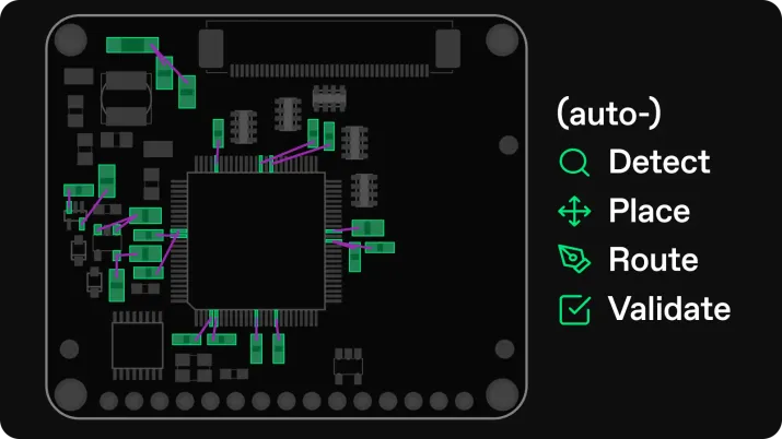
AI-first EDA tools like Quilter generate multiple layout candidates in parallel. Instead of one layout every few weeks, teams can evaluate dozens of candidates in a single day. Engineers set constraints, define the floorplan, and upload their existing CAD files. The AI handles placement and routing based on physics-driven rules.
The result is an abundance of design options, not a scarcity.
Physics-aware automation improves reliability
AI PCB design only works if the outputs are physically correct. Quilter incorporates physics that identify bypass capacitors, controlled impedance nets, differential pairs, and other critical electrical characteristics. This ensures layouts are not just fast but also validated against real world performance expectations.
AI gives engineering teams more bandwidth
When layout bottlenecks vanish, engineering teams can:
- Experiment with multiple architectures faster
- Iterate on mechanical and electrical constraints simultaneously
- Run more design cycles before committing to a prototype
- Catch issues earlier and reduce redesigns
- Increase the entire program’s pace
AI does not replace engineers. It multiplies what they can accomplish.
How does Quilter compare to traditional EDA platforms?
Traditional EDA tools remain essential. Most engineers will continue using Altium, KiCad, EAGLE, or OrCAD for schematic capture and final polish. What has changed is that AI layout automation can now sit in the middle of the workflow and dramatically accelerate it without requiring teams to abandon their existing systems.
Below is a direct comparison of Quilter and the most common legacy platforms.
Overview comparison table
Quilter’s advantages in detail
1. AI driven layout and physics validation
Quilter generates physically aware board layouts using your constraints and native CAD files. Instead of manually placing components and routing traces for weeks, you get ready to review candidates in hours.
2. Parallel design generation
Legacy tools produce one layout at a time. Quilter produces multiple candidates in parallel, each optimized for your constraints. This enables exploration of stackups, board shapes, and routing strategies.
3. Works with your current tools
Quilter is not a replacement for Altium, OrCAD, or KiCad. It integrates with them. You upload your source files and download completed candidates in the same file format. You can run DRC, polish details, and export manufacturing files in whatever EDA your team already uses.
4. Predictable timelines and scalable workflow
Because the AI handles the most time consuming parts of layout, engineering managers can confidently plan schedules. Teams can route more boards in less time without increasing headcount.
5. Cost and scalability
For teams designing many boards per year, AI driven automation reduces the total cost of layout by eliminating delays and manual overhead. Compared to hiring additional layout specialists, the ROI compounds quickly.
If your choice is between a faster version of the old workflow or a faster workflow built for the age of AI, the comparison becomes straightforward.
What results can you expect with an AI first workflow?
Teams adopting AI driven PCB layout consistently report three major outcomes: massive time savings, more design cycles, and higher quality hardware.
1. Time savings that compound across programs
Quilter users typically cut layout time from several weeks down to a few hours per candidate. This allows teams to integrate layout earlier in the design process, catch issues faster, and move forward sooner.
For example, one Quilter customer in aerospace reduced their board bring up cycle by 4 to 6 weeks by eliminating layout bottlenecks. Faster iteration meant more design options, more testing cycles, and a more predictable path to system integration.
2. More iteration leads to better engineering decisions
When layout is no longer the constraint, teams can experiment with:
- Multiple stackups
- Multiple manufacturers
- Multiple form factors
- Multiple floorplans
This abundance of design options changes how teams allocate time. Instead of spending weeks on a single design, teams compare multiple AI generated layouts side by side and choose the best one.
3. Physics validated designs improve confidence
Quilter evaluates each candidate against the full list of physical constraints. Engineers get clear feedback on:
- What is correct
- What is questionable
- What requires further review
This transparency improves design quality while reducing reliance on tribal knowledge or manual checking.
4. Higher productivity across the entire engineering team
Engineers shift effort from manual layout toward higher value tasks such as architecture, simulation, testing, and integration. Managers gain predictability. Programs move faster. And teams report an immediate sense of relief because layout is no longer the bottleneck.
One customer described Quilter as:
“Like adding a full time layout engineer that works at machine speed.”
Here's how to get your team started quickly
If you want to evaluate EDA tools or explore AI driven layout for the first time, follow this step by step approach. It ensures your team makes an informed decision and sees value quickly.
Step 1: Select a representative pilot project
Pick a board that is complex enough to matter but not mission critical. Ideal candidates include:
- Test boards
- Validation hardware
- Interface expansion boards
- High speed subsystems
- Prototypes with tight mechanical constraints
Avoid choosing your most difficult board as the first test. Prove the workflow first.
Step 2: Upload your existing CAD files into Quilter
Quilter accepts native files from Altium, Cadence, Siemens, or KiCad. The process is simple:
- Upload your project.
- Define the board outline.
- Pre place critical connectors.
- Set your constraints.
This part takes less than an hour.
Step 3: Generate multiple layout candidates
Quilter will produce layouts in hours. Use the review interface to compare:
- Physics validation results
- Trace quality
- Placement patterns
- Constraint satisfaction
Choose a candidate that best aligns with your goals.
Step 4: Import back into your existing EDA environment
Once you select a candidate, download the CAD file in the same format you uploaded. Run DRC, adjust small details, and prepare for fabrication as usual.
No workflow disruption. No complicated migration.
Step 5: Gather team feedback
Ask:
- Did this process save time?
- Did the AI produce usable layouts?
- Could this speed help future projects?
- What improvements do we want next?
Most teams find that after a single pilot project, they immediately want to expand usage.
Step 6: Scale the workflow across your organization
Once everyone sees the time savings and quality improvements:
- Apply Quilter to more complex boards
- Integrate it into program planning
- Train new engineers on the constraints workflow
- Create internal playbooks and checklists
- Track time saved and iteration gained
This is how organizations transform their development speed and adopt hardware rich development practices.
Final thoughts and next steps
Choosing EDA software in the age of AI is no longer about which platform offers the most menus or the largest library. It is about which environment helps your team learn faster, build faster, and adapt faster.
Traditional EDA tools remain essential. But AI driven platforms like Quilter are now elevating the entire hardware development process by automating layout, improving design quality, and giving teams more bandwidth.
If you want to see what AI first PCB design looks like for your own team, start with a small pilot and experience the difference firsthand.
Start a free Quilter trial
Schedule a demo with our engineering team
Download the EDA Evaluation Checklist
Your next hardware program can move faster. Your team can iterate more. And bottlenecks that felt unavoidable for years can disappear almost overnight.
Now is the right time to choose EDA software with the future in mind.