

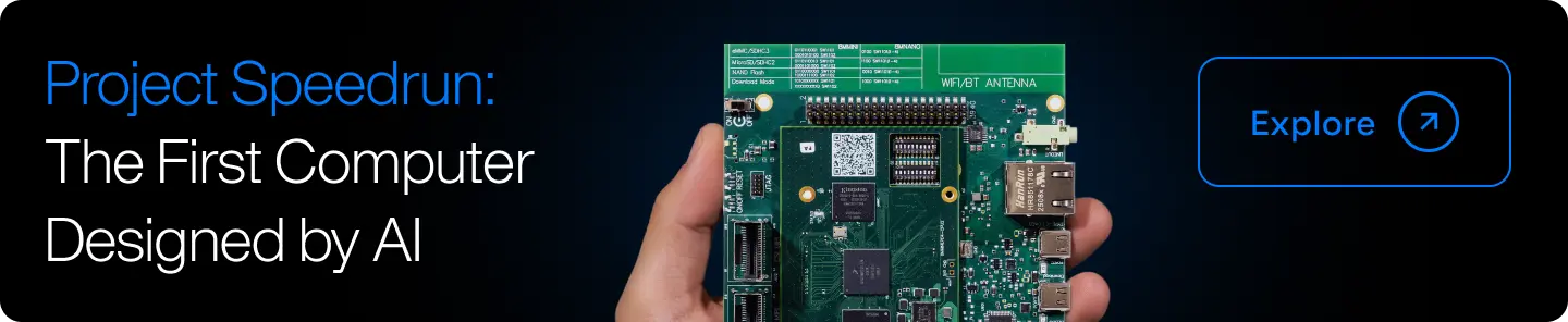


Read the Full Series
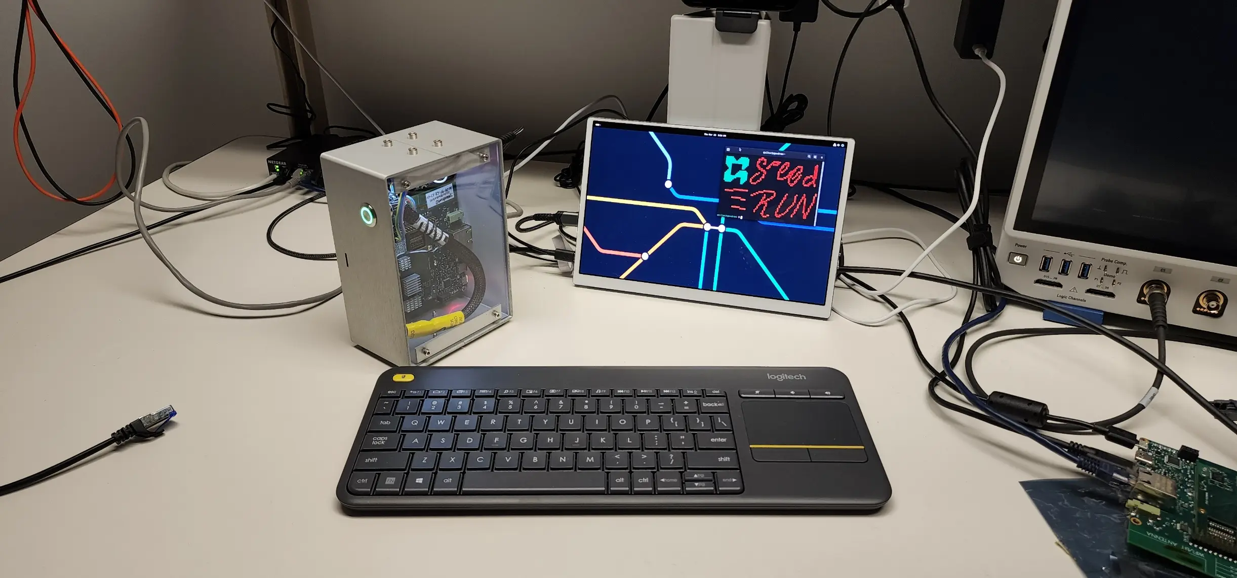
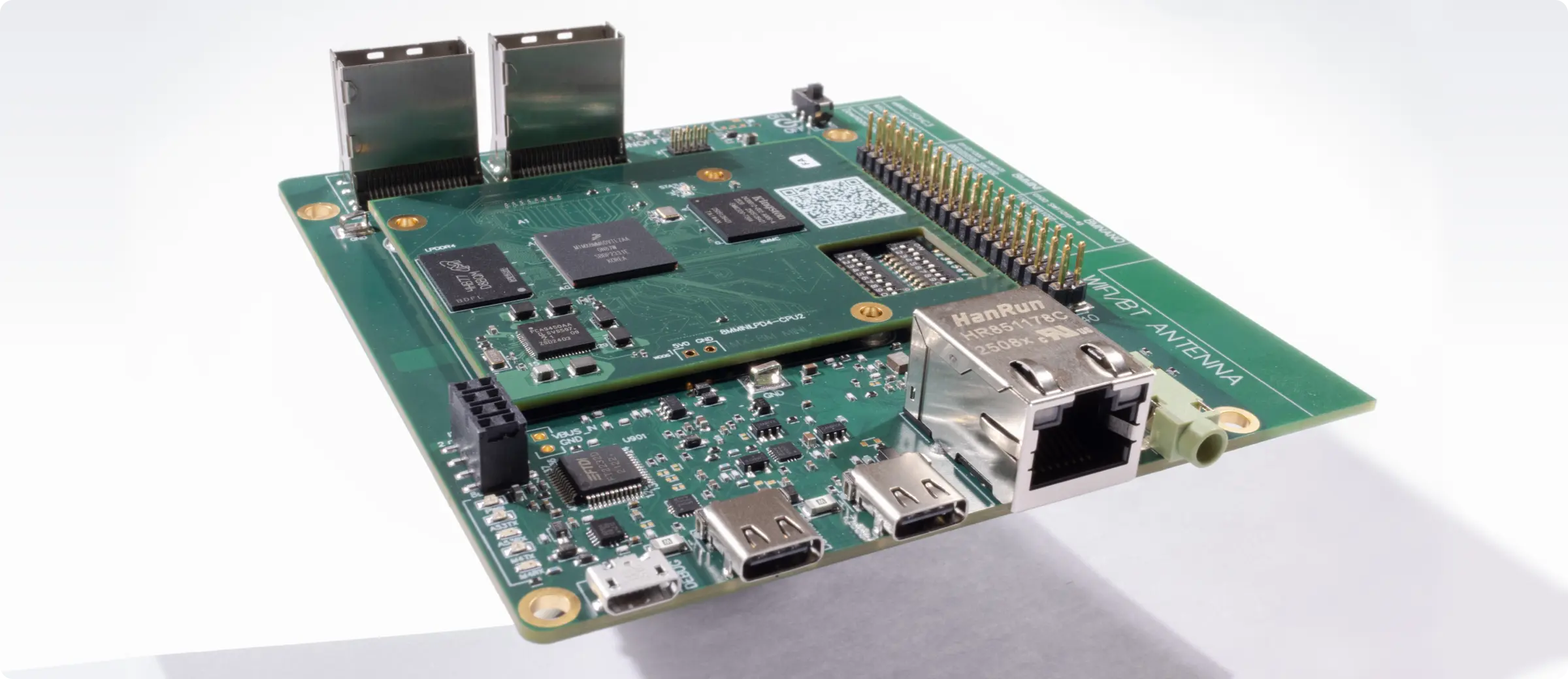
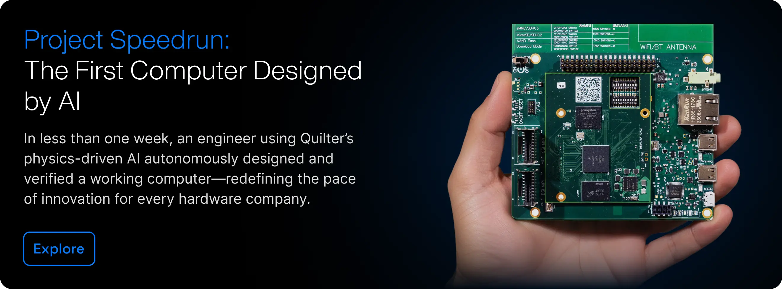
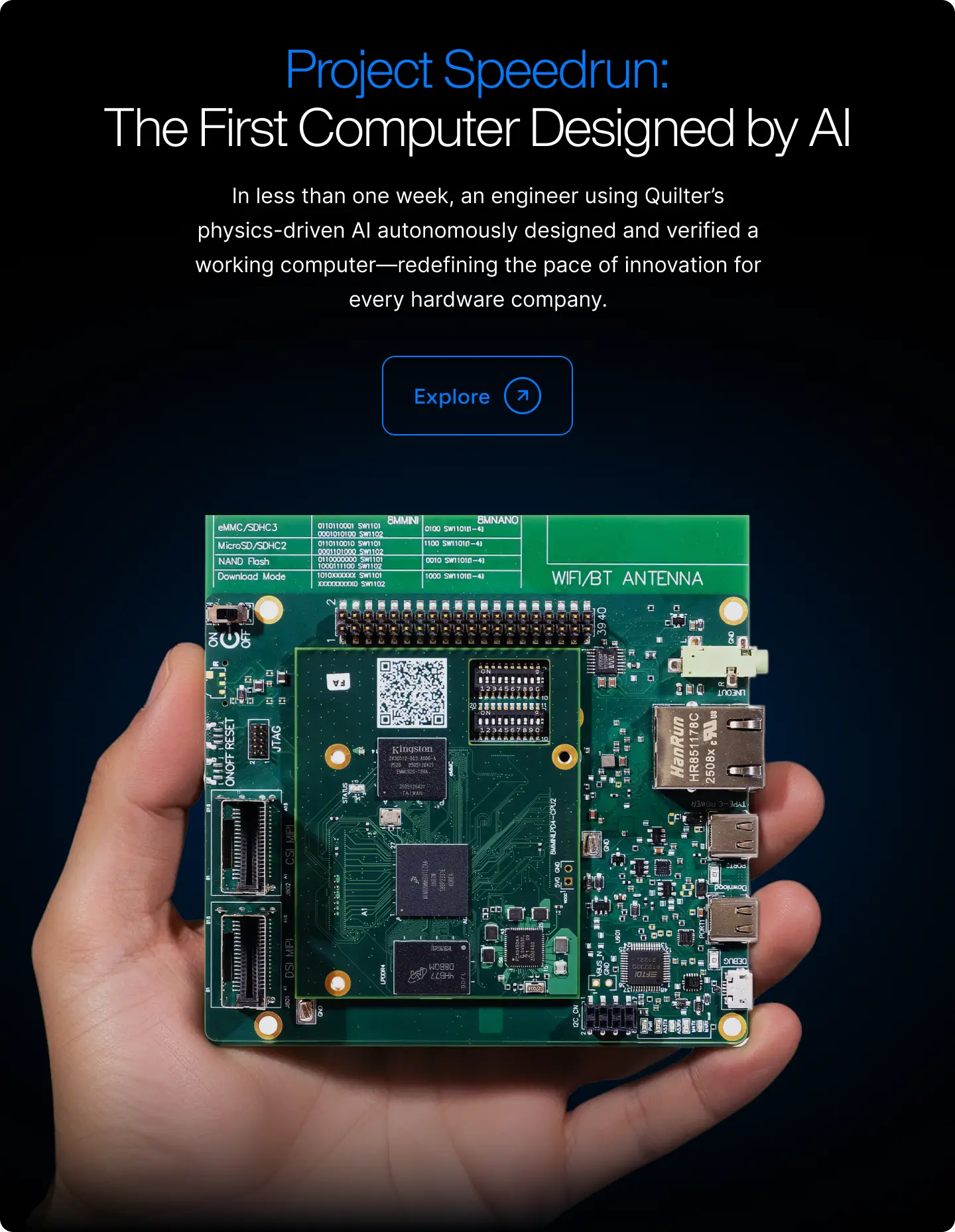
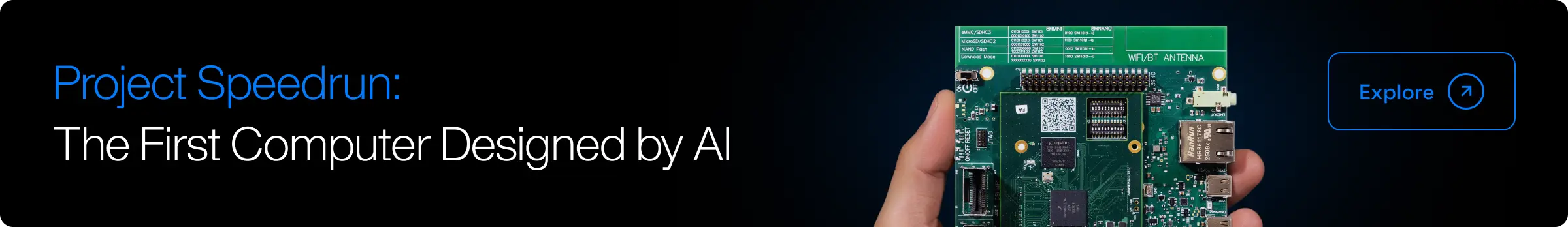
This article is one part of a walkthrough detailing how we recreated an NXP i.MX 8M Mini–based computer using Quilter’s physics-driven layout automation.
Kurz gesagt: Herkömmliche Autorouter maßen ihren Erfolg an der Abschlussrate – also daran, wie viele Netze sie ohne Verletzung der Designregeln verbinden konnten. Doch eine zu 100 % verbundene Platine ist nicht zwangsläufig eine funktionierende Platine. Sie kann den Design Rule Check (DRC) bestehen und dennoch Probleme mit Rückstrompfaden, mangelnder Impedanzkontrolle, übermäßiger Kopplung oder bei der Bestückung aufweisen.
Die wichtigste Lektion aus sechzig Jahren PCB-Layout-Automatisierung lautet: Pins zu verbinden ist nicht dasselbe, wie eine Platine zu erstellen, der ein Ingenieur vertrauen kann.
Die eigentliche Aufgabe eines PCB-Layout-Automatisierungstools besteht darin, den Arbeitsaufwand für eine fertigungsreife Platine zu reduzieren. Um dies zu erreichen, muss die nächste Generation von Tools ein komplexeres Problem lösen: Sie muss Platzierung und Routing als ein zusammenhängendes Problem betrachten, Layout-Kandidaten anhand des elektrischen Verhaltens der fertigen Platine bewerten und genügend Alternativen prüfen, um praktikable Lösungen zu finden.
Angesichts der langen Geschichte von Versuchen, das PCB-Layout zu automatisieren, sind wir uns der Skepsis in der Branche durchaus bewusst. Wir wissen, dass „Ist das wieder so ein Autorouter?“ einer der ersten Gedanken ist, der Ingenieuren in den Sinn kommt, wenn sie zum ersten Mal von Quilter hören.
Dieser Artikel beleuchtet, warum die PCB-Layout-Automatisierung endlich die Grenzen herkömmlicher Autorouter überwinden kann und wie Quilter genau das umsetzt.
Autorouter vs. KI-Layout-Automatisierung im Überblick
Was ist ein PCB-Autorouter?
Ein PCB-Autorouter ist ein Software-Tool, das eine Platine mit bereits platzierten Komponenten nimmt und die Netze dazwischen auf einem Raster und unter Einhaltung bestimmter Vorgaben mit Leiterbahnen verbindet. Die erste Version eines Maze-Routing-Algorithmus wurde 1961 veröffentlicht. Kommerzielle Autorouter wurden in Cadence Allegro, Altium, Siemens Xpedition und von anderen Anbietern integriert. Ingenieure haben ebenso konsequent gelernt, ihnen nicht zu vertrauen.
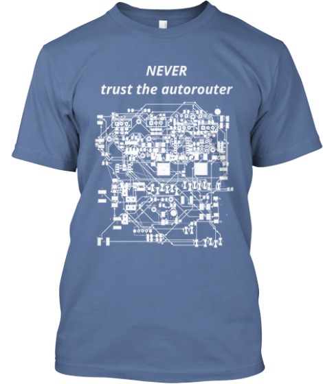
Fragen Sie einen PCB-Designer mit zwanzig Jahren Erfahrung nach Autoroutern, und Sie werden immer dieselbe Geschichte hören: Sie haben ihn eingerichtet, laufen lassen und ein Ergebnis erhalten, das aussah wie Spaghetti, die gegen eine Wand geworfen wurden. Die Nachbearbeitung dauerte länger als ein kompletter Neuanfang, also haben sie ihn abgeschaltet. Manche tragen T-Shirts mit der Aufschrift „never trust the autorouter“. (EEVblog Forum 2014)
Das PCB-Layout kann ein sehr zeitaufwendiger und mühsamer Prozess sein, der oft einen großen Engpass im Hardware-Entwicklungszyklus darstellt. Es ist nur natürlich, dass viele fähige Leute seit Jahrzehnten versuchen, diesen Prozess zu automatisieren. Und wir sind der Meinung, dass es nach wie vor ein Problem ist, das gelöst werden muss.
Wann tauchten die ersten PCB-Autorouter auf?
Die Idee des automatisierten Routings ist älter als viele der Leute, die heute Platinen entwerfen. 1961 veröffentlichte ein Forscher der Bell Labs namens C. Y. Lee einen Maze-Routing-Algorithmus , der einen Pfad zwischen zwei Punkten auf einem Raster finden konnte (Lee 1961). Dies war der Startschuss für ein ganzes Fachgebiet. Kommerzielle Autorouter folgten in den 1970er und 1980er Jahren. Bis 1989 hatten John Cooper und David Chyan Cooper & Chyan Technology gegründet und Specctra auf den Markt gebracht, den formbasierten Router, der zum Industriestandard wurde. Cadence übernahm das Unternehmen 1997 für rund 400 Millionen Dollar – die damals teuerste EDA-Übernahme der Geschichte (Federal Trade Commission 1997; Goering 2005). Eine weiterentwickelte Version von Specctra ist auch heute noch in einigen Cadence-Produkten enthalten.
Der Glaube an diese Idee war tief verwurzelt, selbst bei denjenigen, die ihre Schwächen kannten. 2018 hielt unser Kollege Ben Jordan, damals langjähriger Altium-Ingenieur und Veteran der EDA-Branche, einen viel beachteten Vortrag darüber, ob man dem Autorouter vertrauen kann. Er begann damit, einzuräumen, dass die meisten professionellen Designer, mit denen er gesprochen hatte, keinen Autorouter verwenden würden, argumentierte dann aber, dass es ein Werkzeug sei, dessen Beherrschung sich lohne, anstatt es vorschnell abzuschreiben (Hackaday 2018).
Warum war die Automatisierung des PCB-Layouts schon immer so schwierig?
Layout ist nicht nur ein Problem. Es sind zwei Probleme, die untrennbar miteinander verwoben sind.
Die Platzierung bestimmt, wo jede Komponente sitzt. Das Routing verbindet sie mit Kupfer. Beides ist NP-schwer (Yan et al. 2022). Die Anzahl der Möglichkeiten, eine Platine anzuordnen und zu verdrahten, wächst so schnell, dass der Lösungsraum praktisch unbegrenzt ist.
Die beiden Hälften lassen sich zudem nicht voneinander trennen. Man kann eine Platzierung erst beurteilen, wenn man versucht, sie zu routen. Der klassische Autorouter hat diese Kopplung nie gelöst. Er ging davon aus, dass die Platzierung abgeschlossen war, nahm sie als Eingabe und begann mit dem Verlegen der Kupferbahnen. Wenn das Routing stecken blieb, gab das Tool dem Grundriss des Ingenieurs die Schuld und brach ab.
Schnellere Chips konnten diese Lücke nie schließen. Die Rechenleistung folgte dem Moore'schen Gesetz und verdoppelte sich alle paar Jahre. Doch die Komplexität der Platinen wuchs kombinatorisch, während Dichte und Anforderungen stiegen. Das ursprüngliche iPhone von Apple aus dem Jahr 2007 verwendete zwei gestapelte Platinen, um die Elektronik in das Gehäuse einzupassen. Zehn Jahre später kehrte das iPhone X zum gleichen gestapelten Layout zurück, doch die Substrate im Inneren waren nun Substrat-ähnliche PCBs (SLPs) mit Leiterbahnbreiten von nur 10 bis 15 Mikrometern und Microvias in etwa demselben Durchmesserbereich (TechInsights 2017).
Die Entwicklung verlief überall gleich: in der Luft- und Raumfahrt, Verteidigung, Automobilindustrie, Medizintechnik und Industrieelektronik. Jede Gerätegeneration brachte mehr Lagen, eine dichtere Bestückung und feinere Strukturen mit sich. Jede Lage und jede Vorgabe vervielfacht die Wechselwirkungen, die ein Router abwägen muss, sodass das Problem der Hardware davonlief, selbst als diese immer schneller wurde.
Das Schwierigste ist nicht einmal das Finden eines Pfades. Es ist die Dichte: Leiterbahnen so eng nebeneinander auf einer überfüllten Platine zu platzieren, dass alles passt, während jede einzelne Leiterbahn zudem die elektrischen Anforderungen der Schaltung erfüllen muss.
Das Chip-Routing sieht oberflächlich betrachtet ähnlich aus, basiert jedoch auf einem wesentlich regelmäßigeren Raster. Jede Ebene hat eine bevorzugte Richtung, Leiterbahnen knicken nur im rechten Winkel ab, Vias haben Standardgrößen und Bauteile sind parametrisierte Zellen aus einer Bibliothek. Beim PCB-Routing gibt es diese Regelmäßigkeit nicht. Leiterbahnen können in jedem beliebigen Winkel verlaufen. Bauteile gibt es in tausenden Gehäuseformen mit unterschiedlichen Pin-Mustern, Sperrzonen und Abständen. Via-Typen und Designregeln ändern sich je nach Fertigungsverfahren und Lagenaufbau. Vias sind auf einer Platine zudem ein größeres Problem als auf einem Chip. Auf einer Leiterplatte muss ein Via fast immer drei- bis viermal breiter sein als die Leiterbahnen, die es verbindet. In Silizium ist das Via eine massive Metallstruktur, die etwa so breit ist wie die Leiterbahn, was die automatische Platzierung und das Routing erheblich vereinfacht. Jedes PCB-Via beansprucht viel mehr Platz als die Leitung, die es verbindet, und auf einer dicht bestückten Platine summiert sich dieser Platzbedarf schnell.
Es gibt auch eine menschliche Komponente, und diese ist eine größere Herausforderung, als Außenstehende oft vermuten.
PCB-Designer legen Wert auf das Aussehen einer Platine und bezeichnen das Layout oft als „Kunstwerk“. Von Leiterbahnen wird erwartet, dass sie in 45-Grad-Schritten verlaufen (oktilineares Routing), um einen visuellen Rhythmus beizubehalten, offensichtliche Umwege zu vermeiden und so auszusehen, als hätte sie ein erfahrener Ingenieur gezeichnet. Nichts davon ist eine physikalische Notwendigkeit. Eine Platine mit Leiterbahnen in einem Winkel von 37,4 Grad kann elektrisch genauso gut funktionieren. Die 45-Grad-Gewohnheit ist weitgehend ein Erbe der ECAD-Systeme aus den 1980er Jahren, die kein Routing in beliebigen Winkeln verarbeiten konnten. Diese Einschränkung gibt es längst nicht mehr, aber die Konvention bleibt bestehen.
Das soll nicht heißen, dass der Winkel der Leiterbahnen nie eine Rolle spielt. Bei Hochgeschwindigkeitsplatinen hängt beispielsweise der „Fiber Weave Skew“ davon ab, wie eine Leiterbahn relativ zum Glasfasergewebe des Laminats verläuft. Ein gängiger Weg, dies zu reduzieren, ist es, lange Leiterbahnen in einem 10-Grad-Winkel zu den Platinenachsen zu verlegen (Simonovich 2011). Ein weiteres Beispiel sind Säurefallen. Wenn während des Fertigungsprozesses zwei Leiterbahnen in einem 90-Grad-Winkel aufeinandertreffen, kann die scharfe Innenecke Ätzmittel einschließen. Wenn es dort verbleibt, kann es das Kupfer weiter angreifen, die Leiterbahn verengen oder bei sehr dünnen Leiterbahnen sogar vollständig unterbrechen. Die Säurefalle ist ein Grund, warum Designern beigebracht wurde, spitze Winkel zu vermeiden. Moderne Fertigungsverfahren haben spitze Winkel weniger gefährlich gemacht als früher, aber es ist dennoch etwas, das man mit seinem Fertiger abklären sollte.
Der Hauptgrund, warum Designer bestimmte Ästhetiken bevorzugen, sind jedoch Konvention und Gewohnheit und nicht physikalische Anforderungen. Ein Tool, das dies ignoriert, liefert Ergebnisse, die Ingenieure sofort ablehnen, noch bevor sie prüfen, ob die Schaltung elektrisch einwandfrei ist. Schlimmer noch: Die Ästhetik ist nicht universell. Was „richtig aussieht“, variiert je nach Unternehmen, Team und manchmal sogar je nach individuellem Prüfer.
Was haben traditionelle Autorouter eigentlich getan?
Der klassische Autorouter war eine Sammlung sorgfältig abgestimmter Algorithmen, eingebettet in ein Expertensystem.
Maze-Router fanden ein Netz nach dem anderen und blockierten, wenn spätere Netze denselben Kanal benötigten. Formbasierte Router wie Specctra stellten Hindernisse geometrisch dar und konnten bestehende Leiterbahnen beiseite schieben, um Platz zu schaffen. „Rip-up-and-retry“-Strategien ermöglichten es den Routern, eine frühere Entscheidung rückgängig zu machen und es erneut zu versuchen. Verhandlungsbasierte Router, die von McMurchie und Ebeling (1995) für FPGAs eingeführt wurden, ließen Netze um knappe Ressourcen konkurrieren und iterativ entscheiden, wer was bekommt.
Jedes dieser Elemente war ein Versuch, das Wissen eines guten Designers zu kodieren. Die Art und Weise, wie sie in der Praxis scheiterten, war immer dieselbe und ließ sich auf zwei Punkte reduzieren.
Erstens verwandelte der Autorouter technisches Urteilsvermögen in eine feste Rangfolge von Regeln. Diese Leiterbahnen getrennt halten. Vias minimieren. Diese Ebene für Hochgeschwindigkeitssignale bevorzugen. Stromversorgung zuerst routen. Jede Regel war für sich genommen sinnvoll. Der Haken ist, dass eine Rangfolge eine im Voraus getroffene Vermutung ist. Sie legt eine Abfolge von Kompromissen fest, bevor die erste Leiterbahn verlegt wurde, und das Tool hat keine Möglichkeit, diese zu überdenken, während sich die Platine füllt, da es nie berechnet, wie sich eine bestimmte Entscheidung auf die Schaltung auswirkt. Ein erfahrener Designer ordnet Regeln nicht abstrakt. Er wägt eine spezifische Leiterbahn gegen die vor ihm liegende Platine ab, im Wissen darum, was elektrisch schiefgehen kann. Der Autorouter wandte die Rangfolge starr an und akzeptierte das Ergebnis.
Zweitens optimierte der Autorouter, wie bereits erwähnt, das falsche Ziel. Die standardmäßige interne Metrik war die Abschlussrate: Welcher Prozentsatz der Netze wurde vom Tool ohne Verletzung der Regeln verbunden? Designer wissen, dass dies das falsche Ziel ist; eine geroutete Platine ist nicht dasselbe wie eine produktionsreife Platine. Autorouter hatten kein Verständnis für die Physik der Platine oder die Designabsicht und keine Möglichkeit zu beurteilen, wie sich eine fertige Platine verhalten würde.
Worauf sollte ein Tool zur Automatisierung des PCB-Layouts gemessen werden?
Vollständigkeitsrate, Via-Anzahl und Laufzeit sind wichtig. Sie beweisen jedoch nicht, dass ein erzeugter Layout-Entwurf tatsächlich gut ist. Eine bessere Methode zur Bewertung eines Layout-Automatisierungstools besteht darin, zu prüfen, ob die erzeugten Entwürfe DRC-konform sind, die relevanten physikalischen Anforderungen erfüllen, kritische Rückstrompfade wahren, Impedanzvorgaben einhalten, unnötige Kopplungen vermeiden und den Ingenieur nicht mehr Zeit für die Nachbearbeitung kosten, als wenn er das Layout manuell erstellt hätte.
Der eigentliche Maßstab ist, ob das Tool einen Entwurf liefert, den ein Ingenieur prüfen, dem er vertrauen und auf dessen Basis er weiterarbeiten kann.
Das erste fehlende Puzzleteil: Eine physikalisch fundierte Entscheidungsfindung
Physikalisch fundiert zu entscheiden bedeutet, Layout-Entscheidungen auf Basis des tatsächlichen Schaltungsverhaltens zu treffen und nicht anhand einer starren Regelliste. Autorouter konnten das nie. Um zu wissen, ob eine Routing-Entscheidung die Impedanz einhält, Rückstrompfade bewahrt oder Übersprechen vermeidet, muss die Physik der resultierenden Leiterplatte berechnet werden. Um dies bei den vielen tausend Entscheidungen zu tun, die eine Leiterplatte erfordern kann, benötigt man ein System, das den Suchraum effizient durchlaufen kann: Entscheidungen vorschlagen, Ergebnisse bewerten und aus Erfolgen lernen.
Der naheliegende Ansatz, ein KI-Modell mit bestehenden Leiterplattendesigns zu trainieren, funktioniert aus mehreren Gründen nicht. Erstens gibt es keinen großen, öffentlichen und gut annotierten Datensatz moderner PCB-Designs; die meisten Designs funktionierender Produkte sind als proprietäres geistiges Eigentum in Unternehmen verschlossen. Zweitens sind nicht alle PCB-Designs gleichwertig; Nachahmung übernimmt menschliche Fehler und begrenzt die Ergebnisse auf ein menschliches Niveau.
Hier wird Reinforcement Learning (RL) nützlich. Definieren Sie, wie eine gute Leiterplatte aussieht, generieren Sie viele Entwürfe, bewerten Sie jeden anhand der Physik und lassen Sie das System lernen, welche Entscheidungen zum Ziel führen. Das ist keine Brute-Force-Methode, sondern eine intelligente Suche. Das Modell nutzt Erkenntnisse aus früheren Versuchen, synthetischen Trainingsproblemen und bereits bewältigten Problemklassen, um Sackgassen zu vermeiden und dort Aufwand zu investieren, wo eine Lösung wahrscheinlich ist – genau wie ein erfahrener Designer es tun würde.
Als funktionierende Technologie ist Reinforcement Learning relativ neu. Die Ergebnisse, die es glaubwürdig machten, sind weniger als ein Jahrzehnt alt: AlphaGo im Jahr 2016 und AlphaGo Zero im Jahr 2017.
Das Spiel Go ist ein guter Vergleich zum PCB-Design. Sein Suchraum ist so groß, dass die Baumsuche-Methoden, die in den 1990er Jahren menschliche Schachweltmeister besiegten, bei Go fast zwei Jahrzehnte lang scheiterten – bis DeepMind die Baumsuche mit einem neuronalen Netz kombinierte, das lernte, welche Züge eine Betrachtung wert waren. Das erste AlphaGo lernte dies aus menschlichen Partien. AlphaGo Zero verwarf die menschlichen Daten, lernte durch Selbstspiel allein aus den Regeln und besiegte die menschlich trainierte Version mit 100 zu 0. DeepMind trainierte zum Vergleich auch eine Version mit menschlichen Daten; sie lernte anfangs schneller, stagnierte aber bei schlechteren Ergebnissen (Silver et al. 2017).
Dieser Unterschied ist für das Layout entscheidend. Ein Modell, das darauf trainiert ist, fertige Leiterplatten nachzuahmen, ist durch die Vorlagen begrenzt, von denen es gelernt hat. Gibt man ihm ein Design, das sich von allem in diesem Datensatz unterscheidet, greift es auf das ähnlichste Beispiel zurück, das es kennt – was richtig sein kann, aber nicht muss. Quilter lernt nicht durch das Kopieren von Kundenlayouts oder das Nachahmen fertiger menschlicher Designs. Stattdessen lernt das System aus generierten Versuchen, synthetischen Trainingsproblemen und Klassen von Layout-Herausforderungen. Wenn eingereichte Designs zur Verbesserung des Systems verwendet werden, geschieht dies gemäß den Datennutzungsbedingungen von Quilter, um verallgemeinerte Trainingsprobleme zu generieren, nicht um Designmuster zu reproduzieren (Designs von kommerziellen Kunden werden in unserer Trainings-Pipeline überhaupt nicht verwendet, und Designs, die über die kostenlose Version von Quilter eingereicht werden, dienen lediglich der Generierung synthetischer Trainingsdaten).
Das zweite fehlende Puzzleteil: Eine physikalische Überprüfung während der Layout-Generierung
Reinforcement Learning allein reicht nicht aus.
Ein trainiertes Modell ist gut darin, vielversprechende Entscheidungen vorzuschlagen. Es ist jedoch nicht das richtige Werkzeug, um zu berechnen, ob ein spezifisches Differenzialpaar auf einem bestimmten Lagenaufbau mit einem spezifischen Via-Übergang sein Impedanzziel innerhalb der erforderlichen Toleranz erreicht. Diese Frage erfordert einen Solver, keine Schätzung.
Quilter ist kein KI-Unternehmen, das ein Problem gesucht hat, um KI darauf anzuwenden. Wir haben mit dem Problem begonnen und für jeden Teilbereich die richtigen Werkzeuge ausgewählt. Reinforcement Learning navigiert durch die kombinatorische Suche, aber die vorgeschlagenen Entwürfe werden anhand deterministischer Einschränkungen, Regeln und solver-gestützter Berechnungen überprüft. In diesem Aufbau ist KI nützlich, weil sie nach Entwürfen suchen kann, die Prüfungen bestehen, die ein Ingenieur nachvollziehen kann.
Einige Prüfungen sind geometrischer Natur. Hat die Leiterbahn den Mindestabstand verletzt? Kollidiert Kupfer mit einem Sperrbereich? Hält das Layout die vom Fertiger geforderten Designregeln ein?
Einige Prüfungen sind elektrischer Natur. Entspricht ein impedanzkontrolliertes Netz dem Zielwert des Lagenaufbaus? Überquert ein Differenzialpaar eine Aussparung in der Referenzebene? Bleibt die Kontinuität des Rückstrompfads bei einem Lagenwechsel gewahrt? Führt die Leiterbahnführung zu übermäßiger Kopplung oder einer signifikanten Impedanzdiskontinuität?
Manche Entscheidungen sollten konstruktionsbedingt korrekt sein. Ein Differenzialpaar sollte nicht erst „lernen“ müssen, dass seine beiden Leiterbahnen zusammengehören, oder den Abstand zwischen ihnen erraten müssen. Wo das Ergebnis aus dem Lagenaufbau und dem Impedanzziel berechnet werden kann, nutzt Quilter direkt das solver-gestützte Ergebnis. Dasselbe Prinzip gilt für das gesamte System: Reinforcement Learning dort, wo die Suche schwierig ist; Computergeometrie, wo Geometrie den Suchraum reduzieren kann; klassische Solver, wo Physik berechnet werden muss; und exakte Algorithmen, wo exakte Methoden besser funktionieren als gelernte.
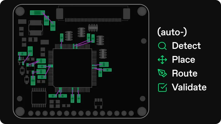
Quilter wendet diese Prüfungen durch Physics Rule Checks (PRCs) an, um sie von den aus herkömmlichen CAD-Tools bekannten DRCs zu unterscheiden. Ein DRC prüft, ob die Geometrie Fertigungs- und Abstandsregeln einhält. Ein PRC prüft, ob der geroutete Entwurf die angestrebten elektrischen Verhaltensvorgaben erfüllt: Masseflächenabdeckung unter Hochgeschwindigkeitsleitungen, Kopplung zwischen Differenzialpaaren, Kontinuität des Rückstrompfads bei Lagenwechseln und Einhaltung der Impedanztoleranz für den Lagenaufbau. Diese Prüfungen laufen während der Generierung des Entwurfs ab, nicht erst nach dem Routing, sodass das System fehlerhafte Layouts verwerfen kann, bevor es sich auf sie festlegt.
Das meinen wir, wenn wir sagen, dass Quilter Leiterplatten kompiliert, anstatt nur Netze zu routen. Der Autorouter hat Pins verbunden. Quilter generiert vollständige Layout-Entwürfe für unterstützte Leiterplattenklassen, wobei gezielte physikalische Prüfungen bereits während der Generierung angewendet werden, anstatt sie vollständig der Überprüfung nach dem Routing zu überlassen.
PRCs sind jedoch keine Garantie für die Einhaltung von EMI/EMC-Richtlinien. Quilter ist ein System für die Platzierung und das Routing von Komponenten, kein Ersatz für menschliche Überprüfung, Inbetriebnahme, Labortests oder regulatorische Konformitätsprüfungen. Quilter folgt zwar Layout-Praktiken, die im Allgemeinen ein besseres elektrisches Verhalten unterstützen – etwa durch die Wahrung einer durchgehenden Massefläche unter Microstrip-Leiterbahnen zur Verbesserung der Signalintegrität –, doch diese Praktiken ersetzen keine nachgelagerten EMV-Tests oder Konformitätsvalidierungen.
Das dritte fehlende Puzzleteil: Rechenleistung in großem Maßstab
Cloud-Computing ist das dritte Puzzleteil.
Specctra und die nachfolgenden Autorouter wurden für den Betrieb auf einer einzelnen Workstation entwickelt. Allegro und Altium liefern ihre Router bis heute auf diese Weise aus. Ein lokaler Router ist auf die Rechenleistung des jeweiligen Computers beschränkt; wenn ein Board komplexer wird, stößt man an Grenzen. Man ist immer auf die Leistung der eigenen Workstation angewiesen.
Diese Obergrenze ist der Hauptgrund dafür, warum Autorouter nie über ein oder zwei erste Versuche hinausgekommen sind. Die Rechenleistung, um den nächsten Kandidaten und die nächsten fünfzig zu testen, war schlicht nicht vorhanden.
Die Cloud hebt diese Beschränkung auf, und die Skalierung ist in dreierlei Hinsicht entscheidend. Erstens muss das Modell trainiert werden, und es lernt aus Millionen von Übungs-Layouts. Zweitens ist der einzig verlässliche Weg, um zu beurteilen, ob eine Platzierung funktioniert, das Routing. Daher muss jede vielversprechende Platzierung, die das Modell ausprobiert, vollständig geroutet werden, um überhaupt in Betracht gezogen zu werden. Drittens muss das System viele Board-Kandidaten gleichzeitig durch Platzierungs-, Routing- und physikalische Prüfungen laufen lassen – ein Arbeitsaufwand, den ein Desktop-Autorouter niemals bewältigen könnte.
Quilter läuft auf der AWS-Cloud-Infrastruktur, wo die Rechenressourcen bei Bedarf automatisch skaliert werden können. Für Teams, die ihre Designs nicht in die Cloud verlagern können – etwa bei ITAR-kontrollierten Projekten oder streng geschütztem geistigem Eigentum –, kann Quilter auch innerhalb Ihrer eigenen AWS-, Azure- oder GCP-Infrastruktur bereitgestellt werden, ohne dass Designdaten Ihr Netzwerk verlassen.
Was können KI-gestützte PCB-Layout-Tools heute leisten?
Nach Jahrzehnten der Fehlstarts ist das automatisierte PCB-Layout einen neuen Blick wert. Nicht, weil das Problem plötzlich gelöst wäre, sondern weil der technologische Fortschritt in anderen Bereichen es endlich ermöglicht, dieses Problem anzugehen. Die oben genannten Punkte bilden das Fundament der heutigen Quilter-Technologie, doch unser Technologie-Stack wird sich weiterentwickeln. Wir haben es uns zur Aufgabe gemacht, das Layout-Problem mit den jeweils besten verfügbaren Werkzeugen zu lösen.
Wir müssen auch transparent über unsere Grenzen sprechen. Quilter gehört zu den fortschrittlicheren Tools auf dem Markt, die das Layout automatisieren, aber wir haben das Problem noch nicht vollständig gelöst. Unser optimaler Einsatzbereich liegt derzeit bei Boards mit 100 bis 1.000 Komponenten, einer Pindichte unter 20 %, Signalen bis etwa 10 GHz und Durchkontaktierungen (Through-Hole Vias). Blind und Buried Vias, BGA-Fanouts, Längenanpassungen und HF befinden sich in unterschiedlichen Entwicklungsstadien. Sie können unseren Fortschritt im Changelogverfolgen. Viele Teams setzen Quilter ein, indem sie es für die Boards, die es gut beherrscht, vollständig durchlaufen lassen und bei komplexeren Boards die Routineabschnitte automatisieren, während sie die kritischen Teile selbst vor-routen.
Quilter entwickelt sich schnell weiter. Der Computer, den wir für Project Speedrun gebaut haben, wäre sechs Monate vor seiner Fertigstellung noch nicht möglich gewesen. Jedes Board, das bei Quilter eingereicht wird, konfrontiert unsere Trainings-Pipeline mit einer neuen Klasse von Problemen. Wir trainieren nicht mit Ihrem Design; wir lernen aus dem Problem, das Ihr Design darstellt. Mehr Nutzer bedeuten schwierigere Probleme. Schwierigere Probleme machen Quilter für alle Nutzer besser.
Die Hardware hat diese Entwicklung bereits bei der Software beobachtet. Softwareentwickler schrieben früher Assembler-Code von Hand und trauten dem Compiler nicht. Die Compiler wurden gut genug, und heute schreibt fast niemand mehr Assembler von Hand, außer in seltenen, spezialisierten Fällen.
Das PCB-Layout befindet sich in einer ähnlichen Anfangsphase. Die Analogie ist nicht perfekt. Boards sind physische Objekte mit Fertigungstoleranzen, Lieferantenvorgaben, Anforderungen an die Signalintegrität und individuellen ästhetischen Vorlieben. Aber die Richtung ist ähnlich: Die Arbeit verlagert sich vom manuellen Zeichnen jedes Details hin zur Definition von Absichten, der Überprüfung von Kandidaten und dem Vertrauen in die Automatisierung für die Bereiche, die sie gut beherrscht.
Der Autorouter war ein Tool zur Netzvervollständigung. Die nächste Generation muss ein Board-Kompilierungssystem sein: ein Werkzeug, das Designabsichten, Randbedingungen, Lagenaufbau, Komponenten und gezielte physikalische Prüfungen entgegennimmt und dann nach vollständigen Layout-Kandidaten sucht, die den tatsächlichen Anforderungen des Boards entsprechen.
Der Autorouter war die richtige Idee für seine Zeit, und das Problem, das er lösen wollte, ist nach wie vor lösenswert. Wir respektieren dieses Erbe und bauen darauf auf.
Häufig gestellte Fragen
Was ist der Unterschied zwischen einem Autorouter und KI-gestütztem PCB-Layout? Ich habe bereits einen Autorouter in meinem EDA-Tool. Warum sollte ich Quilter verwenden?
KI-gestütztes PCB-Layout ist nicht dasselbe wie Autorouting.
Ein herkömmlicher Autorouter betrachtet die Platzierung als festen Input und verbindet Netze mithilfe von gitterbasierten, formbasierten oder topologischen Routing-Methoden. Der Erfolg wird dabei meist an der Abschlussrate gemäß den Designregeln gemessen.
KI-gestütztes PCB-Layout, wie es Quilter entwickelt hat, betrachtet Platzierung und Routing als ein zusammenhängendes Problem. Es nutzt Reinforcement Learning zur Navigation im Suchraum, klassische Solver zur Unterstützung gezielter physikalischer Prüfungen sowie Cloud-basierte oder kundeneigene Rechenleistung, um viele Kandidaten parallel zu untersuchen.
Der entscheidende Unterschied liegt in der Zielsetzung. Der Autorouter versucht, Netze zu verbinden. KI-gestütztes PCB-Layout versucht, vollständige Layout-Kandidaten zu generieren, die nützlich, prüfbar und für die unterstützten Board-Klassen physikalisch valide sind.
Mit anderen Worten: Autorouting ist meist netzorientiert, während KI-gestütztes PCB-Layout eher systemorientiert ist.
Ist Quilter nur ein trainiertes Modell?
Nein. Quilter ist nicht nur ein trainiertes Modell, das Layouts aus Beispielen generiert. Das System kombiniert Reinforcement Learning, Computergeometrie, klassische Solver und exakte Algorithmen. Wo eine Einschränkung direkt gehandhabt werden kann, versucht Quilter, dies „konstruktiv korrekt“ zu lösen, anstatt sich darauf zu verlassen, dass ein Modell dies erlernt. Beispielsweise sollte der Abstand von Differenzpaaren aus dem Lagenaufbau und dem Impedanzziel abgeleitet werden, nicht von einem neuronalen Netzwerk erraten werden.
Lohnt sich der Einsatz von PCB-Autoroutern?
Manchmal.
Autorouter können bei einfachen Boards, unkritischen Verbindungen, explorativem Routing oder als erster Entwurf nützlich sein, wenn der Nachbearbeitungsaufwand gering ist. Sie sind weniger hilfreich, wenn das Board dicht bestückt, hochfrequent, stark eingeschränkt oder empfindlich gegenüber Platzierungs- und Routing-Kompromissen ist, die sich während des Designs ändern.
Die Frage ist nicht, ob ein Autorouter Kupferbahnen verbinden kann. Die Frage ist, ob das Ergebnis Zeit spart oder zusätzliche Arbeit verursacht.
Übernimmt Quilter auch die automatische Platzierung der Komponenten oder nur das Routing?
Quilter übernimmt sowohl die Platzierung als auch das Routing. Wenn Komponenten, Vor-Routings oder Kupferflächen bereits innerhalb der Board-Grenzen platziert sind, kann Quilter diese beibehalten. Komponenten, die sich außerhalb der Grenzen befinden, können automatisch platziert werden, wobei Design-Kontexte wie die Zuweisung von Bypass-Kondensatoren, Gruppierungen von DC-DC-Wandlern, Quarzoszillatoren, die Schaltplanstruktur und Platzierungsbereiche berücksichtigt werden. Das ist ein Grund, warum sich Quilter von einem herkömmlichen Autorouter unterscheidet, der meist davon ausgeht, dass die Platzierung bereits feststeht.
Wie viel Kontrolle habe ich über das Layout?
Sie haben die volle Kontrolle und können Quilter so viel oder so wenig vom Layout übernehmen lassen, wie Sie möchten. Sie können lediglich einen Board-Umriss ohne platzierte Komponenten hochladen und Quilter alles von Anfang bis Ende erledigen lassen. Alternativ können Sie kritische Komponenten vorplatzieren und Netze vor-routen, während Quilter den Rest ausfüllt. Alles, was in der von Ihnen hochgeladenen Board-Datei bereits platziert oder geroutet ist, betrachtet Quilter als „gelöst“ und arbeitet darum herum, ohne Änderungen vorzunehmen.
Zeigt Quilter an, welche Anforderungen erfüllt wurden?
Ja. Quilter liefert Ergebnisse, die Ingenieuren helfen zu verstehen, welche identifizierten Anforderungen erfüllt wurden und welche noch Aufmerksamkeit erfordern. Das ist wichtig, da KI-Layout keine Blackbox sein sollte. Der Designer muss wissen, wo Quilter einen brauchbaren Kandidaten erstellt hat, wo eine menschliche Überprüfung erforderlich ist und wo eine weitere Iteration nötig sein könnte.
Führt Quilter eine EMI/EMC-Verifizierung durch?
Nein. Quilter führt keine EMI/EMC-Konformitätsprüfung durch, und wir behaupten nicht, dass ein nach dem Routing heruntergeladenes Design mit irgendeiner spezifischen EMI/EMC-Regel, Norm oder Zertifizierungsanforderung konform ist.
Quilter ist ein System zur Platzierung und zum Routing von Komponenten. Es nutzt Physik, bestärkendes Lernen (Reinforcement Learning), Solver und klassische Algorithmen, um bessere Layout-Vorschläge zu generieren. Die Verantwortung für die Überprüfung des Designs, die Inbetriebnahme der Platine, deren Test sowie die Entscheidung, ob sie die geltenden Konformitätsanforderungen erfüllt, liegt jedoch weiterhin beim Ingenieur.
Dennoch folgt Quilter im Allgemeinen Layout-Praktiken, die eine bessere Signalintegrität unterstützen, wie etwa die Beibehaltung einer durchgehenden Massefläche unter Mikrostreifenleitungen, wo dies sinnvoll ist. Diese Praktiken können die Qualität der Layout-Vorschläge verbessern, ersetzen jedoch keine nachgelagerten EMI/EMC-Tests oder Konformitätsprüfungen.
Referenzen
EEVblog Forum. 2014. „Chris Gammell's 'Never Trust the Autorouter' Shirt on Teespring.“ Diskussionsthread. https://www.eevblog.com/forum/chat/chris-gammel_s-_never-trust-the-autorouter-shirt_-on-teespring/.
Federal Trade Commission. 1997. „FTC Settlement with Cadence, Cooper & Chyan To Preserve Competition in Automated Chip Design Software.“ Pressemitteilung, 8. Mai 1997. https://www.ftc.gov/news-events/news/press-releases/1997/05/ftc-settlement-cadence-cooper-chyan-preserve-competition-automated-chip-design-software.
Goering, Richard. 2005. „EDA Pioneer Takes Startup to New Routing Ground.“ EE Times, 22. August 2005. https://www.eetimes.com/eda-pioneer-takes-startup-to-new-routing-ground/.
Hackaday. 2018. „Friday Hack Chat: Trusting the Autorouter.“ 21. Februar 2018. https://hackaday.io/event/56777-trusting-the-autorouter/log/100474-trusting-the-autorouter-hack-chat-transcript
Lee, C. Y. 1961. „An Algorithm for Path Connections and Its Applications.“ IRE Transactions on Electronic Computers EC-10 (3): 346–365. https://doi.org/10.1109/TEC.1961.5219222.
McMurchie, Larry und Carl Ebeling. 1995. „PathFinder: A Negotiation-Based Performance-Driven Router for FPGAs.“ In Proceedings of the Third International ACM Symposium on Field-Programmable Gate Arrays, 111–117. https://doi.org/10.1145/201310.201328.
Silver, David, et al. 2017. „Mastering the Game of Go without Human Knowledge.“ Nature 550: 354–359. https://doi.org/10.1038/nature24270.
Simonovich, Bert. 2011. „Fiber Weave-Induced Timing Skew.“ Bert's Practical Design Notes, I-Connect007, 17. September 2011. https://iconnect007.com/article/61693/berts-practical-design-notes-fiber-weaveinduced-timing-skew/61696/design.
TechInsights. 2017. „Apple iPhone X Teardown.“ Blogbeitrag, 13. September 2017, aktualisiert am 8. November 2017. https://www.techinsights.com/blog/apple-iphone-x-teardown.
Yan, Junchi, Xianglong Lyu, Ruoyu Cheng und Yibo Lin. 2022. „Towards Machine Learning for Placement and Routing in Chip Design: A Methodological Overview.“ arXiv preprint arXiv:2202.13564. https://arxiv.org/abs/2202.13564.