






Die gesamte Serie lesen
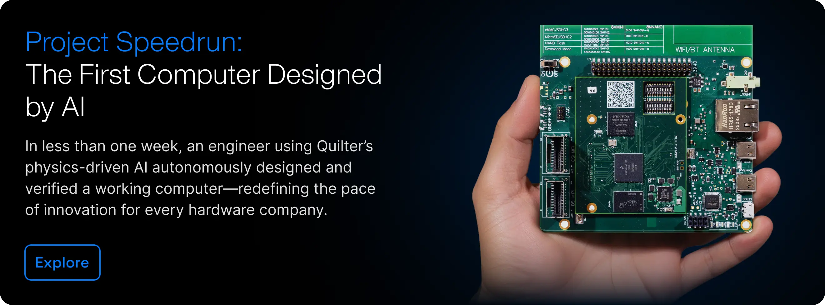
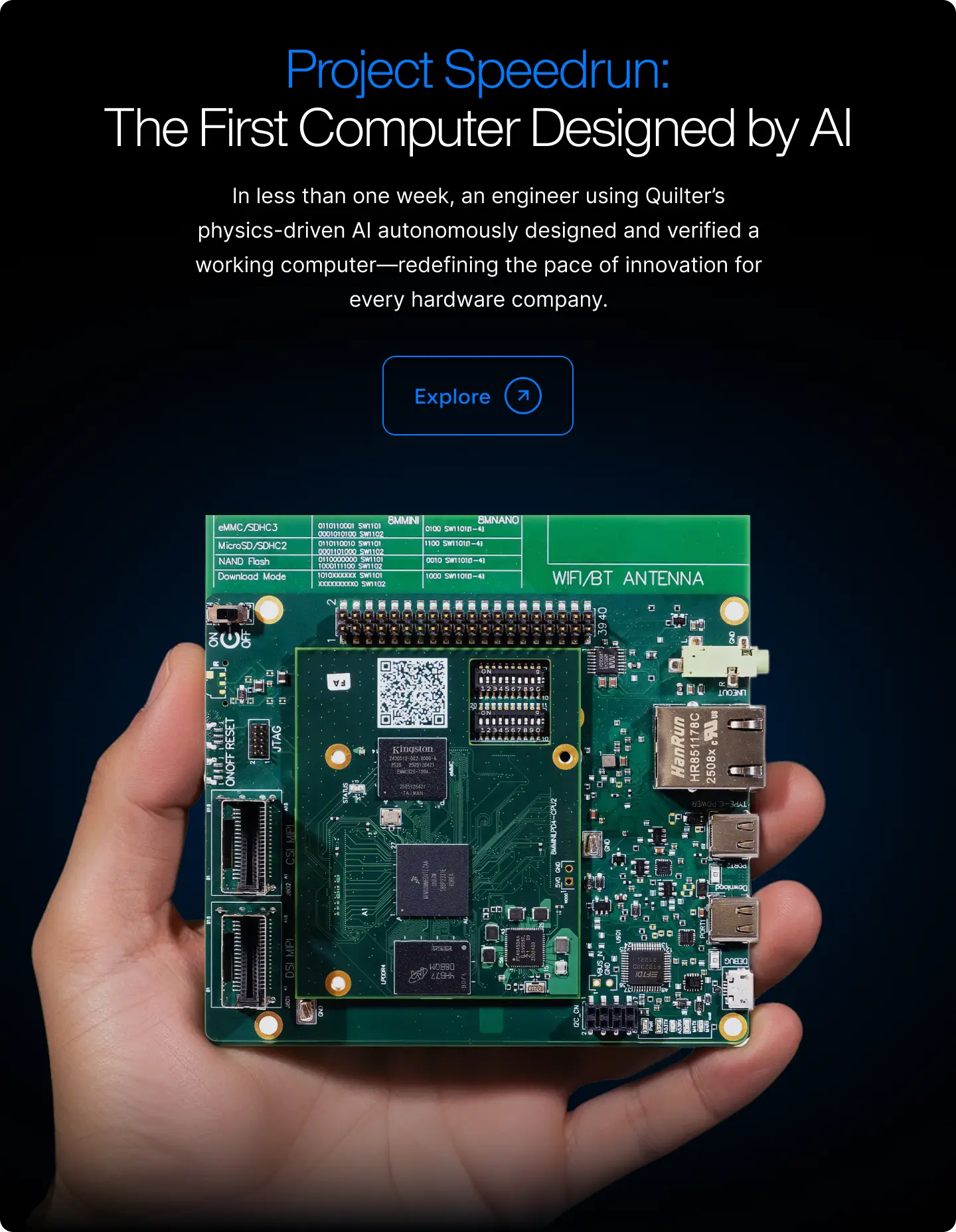
Dieser Artikel ist Teil einer ausführlichen Anleitung dazu, wie wir mit Quilters physikgestützter Layout-Automatisierung einen Computer auf Basis des NXP i.MX 8M Mini nachgebaut haben.
PCB-Autorouting wandelt sich, weil sich die Hardware wandelt
PCB-Autorouting wandelt sich, weil sich die Hardware wandelt. Ältere Routing-Tools wurden für eine engere Definition des PCB-Layout-Problems entwickelt: ein bestücktes Board nehmen, so viele Netze wie möglich verbinden, offensichtliche Design-Regelverstöße vermeiden und dem Ingenieur ein Ergebnis liefern, das manuell fertiggestellt werden kann.
Das war für die damalige Zeit ein vernünftiges Ziel. Es war jedoch unvollständig.
Modernes PCB-Layout stellt komplexere Anforderungen. Kann ein Tool einen Board-Entwurf generieren, den ein Ingenieur prüfen, dem er vertrauen, den er fertigen und in Betrieb nehmen kann, ohne tagelang die Arbeit des Tools korrigieren zu müssen? Die Vollständigkeit ist nach wie vor wichtig, aber sie allein beweist nicht, dass ein geroutetes Board elektrisch einwandfrei funktioniert. Ein Board kann den Design Rule Check bestehen und dennoch unterbrochene Rückstrompfade, eine schlechte Impedanzkontrolle, vermeidbare Kopplungen, ungünstige Platzierungskompromisse, problematische Fertigungsaspekte oder ein Routing aufweisen, das zwar technisch funktioniert, das Design aber verschlechtert.
Jede Generation von Routing-Tools spiegelt die Annahmen ihrer Zeit wider. Sobald sich Board-Dichte, Datenraten, Fertigungsregeln, Gehäuseformen und systemweite Anforderungen weiterentwickeln, stoßen ältere Annahmen an ihre Grenzen. PCB-Autorouting ist nicht gescheitert, weil es den Ingenieuren an Vorstellungskraft mangelte. Es ist nach wie vor schwierig, weil sich die Definition eines „guten Routings“ ständig erweitert.
Was ist das Problem beim PCB-Autorouting?
Das PCB-Autorouting-Problem besteht darin, automatisch ein gültiges, effizientes und fertigungsgerechtes Routing für eine Leiterplatte zu generieren und dabei elektrische, physische, abstandsbezogene, zeitliche und regelbasierte Anforderungen zu erfüllen. Nach altem Verständnis erhielt ein Autorouter ein bestücktes Board und versuchte, die Netze mit Kupferbahnen zu verbinden. Der Erfolg wurde meist an der Abschlussrate gemessen: wie viele Netze ohne Verletzung der vorgegebenen Regeln geroutet werden konnten.
Dieser Ansatz war sinnvoll, als die Hauptaufgabe des Tools in der Konnektivität bestand. Eine Verbindung war entweder vorhanden oder nicht. Eine Leiterbahn verletzte entweder den Mindestabstand oder nicht. Ein Netz war entweder vollständig oder unvollständig.
Im modernen PCB-Design können Teams Routing nicht mehr als reine Konnektivität betrachten. Ingenieure müssen heute Rückstrompfad-Kontinuität, kontrollierte Impedanz, das Verhalten von Differenzpaaren, Kopplungen, Vias, Layer-Übergänge, Breakout-Dichte, Stromverteilung, thermisches Verhalten, Kosten, Fertigungsgrenzen und die Frage berücksichtigen, ob das Board die Prüfung durch einen erfahrenen Experten bestehen wird. Ein vollständig geroutetes Board kann dennoch ein schlechtes Routing aufweisen. Ein zu 100 % geroutetes Board kann immer noch ein Produkt sein, das niemand ausliefern möchte.
Genau dieser Unterschied steht im Mittelpunkt des Problems. PCB-Autorouting bedeutet nicht einfach nur „Pfade zwischen Pins finden“. Es bedeutet „Pfade zwischen Pins finden und dabei das Verhalten, die Anforderungen und die Absicht des physischen Endsystems bewahren“.
Warum herkömmliche PCB-Autorouter bei modernem High-Speed-Design scheitern
Herkömmliche Autorouter haben Schwierigkeiten, weil sie auf veralteten Annahmen darüber basieren, was das Routing-Problem eigentlich ist. Viele traditionelle Router wurden darauf optimiert, die Abschlussrate, die Anzahl der Vias, die Pfadlänge, Abstände und andere regelbasierte Prioritäten zu verbessern. Diese Prioritäten sind nützlich, erfassen aber nicht das gesamte technische Urteilsvermögen, das ein Layout-Designer beim Routing eines modernen Boards anwendet.
Ältere Autorouter konnten zwar Netze verbinden, lieferten aber oft Ergebnisse, die unübersichtlich waren. Ingenieure ließen das Tool laufen, prüften das Ergebnis und stellten fest, dass die Nachbearbeitung länger dauerte als das manuelle Routing. Diese Erfahrung führte zu der bekannten Skepsis in der Branche gegenüber Autoroutern: Das Tool konnte zwar Kupferbahnen erzeugen, aber der Ingenieur musste dennoch entscheiden, ob diese Bahnen sinnvoll waren.
High-Speed-Design macht diese Schwäche noch deutlicher. Sobald die Flankensteilheit zunimmt und sich Verbindungen weniger wie ideale Drähte verhalten, gewinnen Layout-Entscheidungen an elektrischer Bedeutung. Der Verlauf einer Leiterbahn, die Referenzebene, Via-Übergänge, Abstände und die umgebende Geometrie beeinflussen das Verhalten. Das Tool kann nicht erfolgreich sein, wenn es diese Anforderungen nur als zweitrangig betrachtet. Es muss die Physik des Boards ausreichend verstehen, um keine Entwürfe zu generieren, die zwar regelkonform aussehen, aber schlecht funktionieren.
PCB-Autorouting hat sich gewandelt, weil die Abschlussrate das falsche Ziel war
Ältere Tools sind nicht nur veraltet, weil die Hardware komplexer wurde. Sie waren auch auf das falsche Ziel optimiert.
Die Abschlussrate fragt nur, ob der Autorouter das Board verbunden hat. Ingenieure müssen jedoch wissen, ob das Ergebnis den Arbeitsaufwand reduziert, um zu einem fertigungsgerechten, prüfbaren und elektrisch zuverlässigen Design zu gelangen. Das sind zwei völlig unterschiedliche Maßstäbe.
Ein herkömmlicher Autorouter feiert vielleicht eine Leiterplatte mit 95 % gerouteten Netzen. Ein Layout-Ingenieur sieht darin eine Woche Nacharbeit. Das Tool hat seine interne Metrik optimiert. Der Ingenieur beurteilt das tatsächliche Arbeitsergebnis.
Diese Diskrepanz erklärt jahrzehntelange Frustration. Ein Routing-Tool, das ein „fast fertiges“ Layout liefert, kann dennoch versagen, wenn die verbleibende Arbeit schwierig, unübersichtlich und risikobehaftet ist. Ein Tool, das technisch alle Netze verbindet, kann ebenfalls scheitern, wenn das Design umfangreiche manuelle Korrekturen erfordert, bevor man ihm vertrauen kann. Der richtige Maßstab ist nicht, ob der Autorouter Kupferbahnen verbinden kann. Der richtige Maßstab ist, ob das Ergebnis Zeit spart und gleichzeitig das für das Design erforderliche Verhalten der Leiterplatte bewahrt.
Funktionales Routing ist nicht gleichbedeutend mit gutem PCB-Layout
Ein funktionales PCB-Routing verbindet die Netze und erfüllt den vorgegebenen Regelsatz. Ein gutes PCB-Layout spiegelt die Designabsicht wider.
Dieser Unterschied ist wichtig, da erfahrene PCB-Designer nicht nur in lokalen Regeln denken. Sie wägen spezifische Kompromisse im Kontext ab. Sie verstehen, wann eine etwas längere Leiterbahn akzeptabel ist, wann sich ein zusätzliches Via lohnt, wann ein Lagenwechsel ein Risiko für den Rückstrompfad darstellt, wann die Platzierung das Routing in eine Sackgasse geführt hat und wann ein scheinbar sauberer Pfad zu Problemen bei Signalintegrität (SI), Power Integrity (PI), Thermik oder Fertigung führen wird.
Herkömmliche Autorouter haben dieses Urteilsvermögen oft in starre Regelhierarchien umgewandelt. Vias minimieren. Leiterbahnen voneinander fernhalten. Bestimmte Lagen bevorzugen. Bestimmte Netze zuerst routen. Überlastung vermeiden. Jede Regel mag für sich genommen sinnvoll sein, aber eine feste Prioritätenliste kann sich nicht so anpassen wie ein Ingenieur, während die Leiterplatte gefüllt wird. Regeln interagieren miteinander. Entscheidungen, die früh gut aussehen, können später schlechte Kompromisse erzwingen. Ein Routing, das eine Metrik optimiert, kann eine andere verschlechtern.
Moderne Layout-Automatisierung benötigt ein umfassenderes Ziel. Sie muss Kandidaten generieren, die für die menschliche Überprüfung nützlich sind, nicht nur geometrisch vollständig.
PCB-Autorouting hängt auch von der Platzierung ab
Platzierung und Routing werden oft getrennt diskutiert, da ältere Tool-Workflows sie separat behandelten. Erst die Komponenten platzieren. Dann die Netze routen. Dieser Workflow ist vertraut, verbirgt aber einen der schwierigsten Aspekte des Problems.
Man kann eine Platzierung erst dann vollständig beurteilen, wenn man versucht, sie zu routen.
Eine Komponentenplatzierung, die organisiert aussieht, kann eine unmögliche Routing-Dichte erzeugen. Eine Platzierung, die kompakt erscheint, kann Hochgeschwindigkeitsnetze zu ungünstigen Lagenwechseln zwingen. Eine Platzierung, die mechanische Anforderungen erfüllt, kann Probleme bei der Stromverteilung verursachen. Eine Platzierung, die eine Schnittstelle begünstigt, kann einer anderen schaden.
Herkömmliche Autorouter akzeptierten die Platzierung meist als festen Input. Wenn das Routing schwierig wurde, hatte der Router nur begrenzte Möglichkeiten, die Platzierungsentscheidungen zu überdenken, die das Problem überhaupt erst verursacht hatten. Ingenieure mussten dann interpretieren, ob der Router versagte, weil der Routing-Algorithmus schwach war, die Leiterplatte übermäßig eingeschränkt war oder die Platzierung das Problem unnötig erschwerte.
Die Zukunft der PCB-Layout-Automatisierung kann Platzierung und Routing nicht ewig als getrennte Probleme behandeln. Bessere Tools müssen sie als gekoppeltes System lösen. Sie müssen Board-Kandidaten untersuchen, diese routen, bewerten und lernen, welche Kombinationen aus Platzierung und Routing glaubwürdige Ergebnisse liefern.
High-Speed-PCB-Constraints machen Routing zu einem Systemproblem
Bei niedrigen Geschwindigkeiten sind viele Routing-Fehler lediglich unschön oder ineffizient. Bei hohen Geschwindigkeiten wird das Layout Teil der Schaltung.
Differenzielle Paare benötigen Abstände, die dem Lagenaufbau und dem Impedanzziel entsprechen. High-Speed-Leiterbahnen benötigen geeignete Referenzebenen. Lagenwechsel erfordern eine kontinuierliche Rückstromführung. Dichte Breakout-Bereiche erzeugen Routing-Druck. Entscheidungen bei der Stromverteilung beeinflussen Rauschen und Verhalten. Thermische Vorgaben verändern die Komponentenplatzierung und Kupferentscheidungen. Fertigungsvorgaben bestimmen die Wahl der Vias, Leiterbahnbreiten, Abstände und die Lagennutzung.
Keine Routing-Engine kann diese Aspekte als unabhängige Boxen behandeln. Sie beeinflussen sich gegenseitig. Eine Via-Entscheidung kann Dichte, Rückstrompfad, Impedanzdiskontinuität und Fertigbarkeit beeinflussen. Eine Platzierungsentscheidung kann sich auf die Leitungslänge, Stromversorgung, Montage und thermische Leistung auswirken. Eine Lagenwahl kann ein Netz verbessern, während sie für ein anderes zu Engpässen führt.
Moderne automatisierte PCB-Designs benötigen daher einen breiteren technischen Kontext. Ein Tool, das nur eine eingeschränkte Sicht auf das Routing optimiert, wird Teams, denen das gesamte Board am Herzen liegt, weiterhin enttäuschen.
Warum das Bestehen von DRC nicht ausreicht
Design Rule Checks sind notwendig. Sie sind nicht hinreichend.
Ein DRC kann Ingenieuren mitteilen, ob Kupferabstände, Freiräume, Leiterbahnbreiten, Sperrflächen und andere fertigungsorientierte Vorgaben verletzt werden. Das ist essenziell, doch ein DRC beweist nicht, dass sich eine geroutete Platine elektrisch einwandfrei verhält. Eine Platine kann den DRC bestehen und dennoch unter Diskontinuitäten im Rückstrompfad, schlechter Impedanzkontrolle, unerwünschter Kopplung, vermeidbaren Stubs, ungünstigen Übergängen an Referenzebenen oder Layout-Entscheidungen leiden, die die Inbetriebnahme unnötig erschweren.
Die Unterscheidung zwischen DRCs und physikalischen Regelprüfungen ist wichtig, da die Branche Regelprüfungen bereits als Methode zur Geometrieverifizierung versteht. Der nächste Schritt besteht darin, zu prüfen, ob generierte Entwürfe während der Layout-Erstellung – und nicht erst nach Abschluss des Routings – die angestrebten elektrischen Verhaltensvorgaben erfüllen.
Physikbasierte Automatisierung verändert die Feedbackschleife. Anstatt erst zu routen und Probleme später zu entdecken, kann das Tool Entwürfe während der Suche gegen relevante Verhaltensvorgaben bewerten. Schlechte Entwürfe können frühzeitig verworfen werden. Bessere Entwürfe erhalten mehr Rechenleistung. Ingenieure können die Ergebnisse mit einem klareren Verständnis darüber prüfen, welche Vorgaben erfüllt wurden und welche noch Aufmerksamkeit erfordern.
KI-PCB-Layout ist nur dann sinnvoll, wenn es das Ziel verändert
KI repariert das PCB-Autorouting nicht automatisch.
Ein Modell, das darauf trainiert wurde, bestehende Layouts zu imitieren, reproduziert möglicherweise alte Gewohnheiten, übernimmt menschliche Fehler und versagt, wenn sich die nächste Platine von den gesehenen Beispielen unterscheidet. Ein neuronales Netz kann plausible Vorschläge machen, aber Plausibilität ist nicht gleichbedeutend mit Physik. Der Abstand von Differenzpaaren sollte auf Stackup- und Impedanzvorgaben basieren, nicht auf einem Modell, das rät, welcher Abstand „richtig aussieht“. Die Kontinuität des Rückstrompfads sollte anhand des tatsächlichen Layout-Entwurfs geprüft und nicht aus einem Muster abgeleitet werden.
KI wird nützlich, wenn sie hilft, einen riesigen Suchraum zu durchlaufen, während andere Methoden verifizieren, was direkt berechnet werden muss. Reinforcement Learning kann helfen, vielversprechende Entscheidungen vorzuschlagen. Klassische Solver können die Physik prüfen. Computergeometrie kann den Suchraum für das Routing verkleinern. Exakte Algorithmen können Vorgaben handhaben, bei denen deterministische Methoden besser funktionieren als gelernte.
Der entscheidende Wandel ist nicht „KI statt Autorouting“. Der entscheidende Wandel ist ein System, das nach vollständigen, überprüfbaren Platinenentwürfen sucht, die an einem stärkeren Ziel ausgerichtet sind. KI rechtfertigt ihren Einsatz nur dann, wenn sie dabei hilft, Layouts zu erstellen, denen Ingenieure schneller vertrauen können als bei reiner manueller Arbeit.
Multi-Physik gehört in die Diskussion über PCB-Routing
PCB-Routing kann nicht isoliert vom restlichen Platinenverhalten betrachtet werden. Moderne Hardware-Teams wissen das bereits aus der Praxis. Signalintegrität, Power-Integrität, Fertigbarkeit, Thermik, mechanische Gehäuse, Kosten und Montage – all das trifft im Layout aufeinander.
Je stärker Platinen eingeschränkt sind, desto weniger sinnvoll ist es, so zu tun, als sei Routing nur ein Geometrieproblem. Layout-Entscheidungen können Wärme, Rauschen, Timing, Kosten und Ausbeute beeinflussen. Ein Routing-Tool, das diese Konsequenzen ignoriert, mag zwar die Netze fertigstellen, wird aber nicht zuverlässig die Platine produzieren, die ein Engineering-Team tatsächlich benötigt.
Bessere Automatisierung erfordert eine bessere Modellierung von Vorgaben. Tools müssen mehr vom Systemkontext erfassen, nicht weniger. Sie müssen verstehen, welche Vorgaben harte Anforderungen sind, welche Kompromisse flexibel sind, welche Teile des Layouts ein Mensch beibehalten möchte und welche Entwürfe eine weitere Untersuchung verdienen.
Cloud-Computing verändert das Routing-Problem
Herkömmliche Autorouter liefen meist auf einer lokalen Workstation und erzeugten jeweils einen Hauptentwurf. Dieses Rechenmodell prägte das Verhalten der Tools. Eine komplexe Platine benötigte nicht einfach nur einen etwas besseren Pfadfindungsalgorithmus. Oft mussten viele Platzierungs- und Routing-Varianten untersucht, bewertet, verworfen und verbessert werden.
Cloud-Computing verändert, was Layout-Automatisierung leisten kann. Ein System kann mit großen Mengen generierter Layout-Probleme trainiert werden, viele Entwürfe parallel untersuchen, vollständige Platinenentwürfe bewerten und kontinuierlich aus verschiedenen Routing-Herausforderungen lernen. Es geht nicht um Brute-Force um seiner selbst willen. Es geht darum, dem Tool genügend Suchkapazität zu geben, um praktikable Entwürfe in einem Raum zu finden, der für einen einzelnen lokalen Autorouter-Durchlauf zu groß ist.
PCB-Layout hat einen kombinatorischen Charakter. Mehr Komponenten, mehr Lagen, mehr Vorgaben und eine höhere Dichte lassen die Anzahl möglicher Entscheidungen weit schneller anwachsen, als ein Mensch sie erschöpfend prüfen könnte. Ingenieure bewältigen dies durch Erfahrung, Vereinfachung, Mustererkennung und Urteilsvermögen. Automatisierung benötigt ihre eigene Version dieser Fähigkeiten: breite Exploration, gezielte Bewertung und schnelles Verwerfen schlechter Pfade.
Warum ausgereifte EDA-Workflows Veränderungen erschweren
Routing-Innovationen haben auch ein Workflow-Problem. Ausgereifte EDA-Umgebungen sind voll von etablierten Gewohnheiten, Dateiformaten, Tool-Erwartungen, Kundenvorgaben und organisatorischem Wissen. Ingenieure haben gelernt, wo bestehende Tools nützlich sind, wo sie versagen und wie man sie umgeht. Unternehmen benötigen Kompatibilität. Teams benötigen Überprüfbarkeit. Niemand möchte ein Black-Box-System, das eine Platine verändert, ohne zu erklären, was passiert ist.
Diese Realität verlangsamt die Einführung, selbst wenn ein neuer Ansatz technisch stärker ist. Ingenieure fragen nicht nur, ob ein Tool Arbeit automatisieren kann. Sie fragen, ob es in ihren Designprozess passt, die Kontrolle bewahrt, Vorgaben klar offenlegt und Ergebnisse liefert, die sie in ihrer nativen ECAD-Umgebung prüfen können.
Die nächste Generation der PCB-Layout-Automatisierung muss dies respektieren. Ingenieure benötigen die Möglichkeit, kritische Komponenten vorab zu platzieren, bewährte Routings beizubehalten, sensible Bereiche einzuschränken, Scorecards für Entwürfe zu prüfen und zu entscheiden, wo menschliches Urteilsvermögen weiterhin erforderlich ist. Bessere Automatisierung sollte die Arbeit des Ingenieurs vom Zeichnen jedes Details hin zum Definieren von Absichten, Überprüfen von Entwürfen und schnellerem Iterieren verlagern.
PCB-Autorouting entwickelt sich in Richtung Board-Kompilierung
Eine treffende Beschreibung für diesen Wandel ist der Übergang vom reinen Netz-Routing zur Board-Kompilierung.
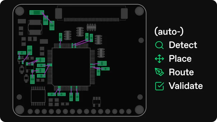
Herkömmliches Autorouting versuchte, Netze nach der Platzierung zu verbinden. Die Board-Kompilierung hingegen berücksichtigt Designvorgaben, Constraints, Lagenaufbau, Komponenten, Platzierungsbereiche, bestehende Routings sowie gezielte physikalische Prüfungen, um dann vollständige Layout-Kandidaten zu finden, die den tatsächlichen Anforderungen der Leiterplatte entsprechen.
Der Vergleich mit einem Compiler ist nicht perfekt, da Leiterplatten physische Objekte sind. Fertigungstoleranzen, Lieferantenvorgaben, Signalintegrität, Inbetriebnahme im Labor und individuelle Layout-Präferenzen spielen eine wichtige Rolle. Dennoch geht die Entwicklung in eine ähnliche Richtung. Ingenieure misstrauten einst Compilern für Aufgaben, die sie zuvor manuell erledigten. Mit der Zeit wurden Compiler für die meisten Routineaufgaben zur vertrauenswürdigen Standardlösung, während der Mensch die Kontrolle über spezialisierte, kritische Fälle behielt. Das PCB-Layout könnte einen vergleichbaren Weg einschlagen: Die Automatisierung übernimmt zunehmend Routineaufgaben und eingeschränkte Prozesse, während sich Ingenieure auf Designabsicht, Überprüfung, kritische Entscheidungen und Validierung konzentrieren.
Der Autorouter war für seine Zeit der richtige Ansatz, doch das Ziel war zu eng gefasst. Moderne Hardware benötigt Werkzeuge, die glaubwürdige Board-Kandidaten optimieren und nicht nur Netze verbinden.
FAQ: PCB-Autorouting, KI-gestütztes PCB-Layout und klassische Autorouter
Warum scheitern alte PCB-Autorouter bei modernen Designs?
Alte PCB-Autorouter scheitern oft daran, dass sie eine zu eng gefasste Version des Layout-Problems optimieren, die den Anforderungen moderner Teams nicht mehr gerecht wird. Sie verbinden zwar viele oder alle Netze, erzeugen aber Layouts, die zu viel Nacharbeit erfordern, wichtige elektrische Eigenschaften ignorieren oder die Designabsicht des Ingenieurs nicht widerspiegeln.
Ist PCB-Autorouting nur ein Problem der Pfadfindung?
Nein. PCB-Autorouting umfasst zwar die Pfadfindung, aber modernes Layout beinhaltet auch Signalintegrität, Power-Integrität, Fertigbarkeit, Kosten, thermisches Verhalten, Rückstrompfade, Impedanzkontrolle, Kopplung, Abwägungen bei der Platzierung und Prüfbarkeit.
Was ist der Unterschied zwischen Autorouting und KI-gestütztem PCB-Layout?
Ein klassischer Autorouter betrachtet die Platzierung meist als festen Input und routet Netze gemäß Designregeln. KI-gestütztes PCB-Layout hingegen betrachtet Platzierung und Routing als zusammenhängendes Problem, untersucht zahlreiche Layout-Kandidaten und prüft diese gegen gezielte physikalische und elektrische Constraints.
Warum ist die Abschlussrate eine schlechte Kennzahl für PCB-Autorouting?
Die Abschlussrate gibt Ingenieuren lediglich an, wie viele Netze verbunden wurden. Sie sagt nichts darüber aus, ob die Leiterplatte fertigungsgerecht, elektrisch einwandfrei, leicht zu prüfen oder schneller fertigzustellen ist als bei manuellem Routing. Ein vollständig geroutetes Board kann dennoch ein schlechtes Layout sein.
Wird KI PCB-Layout-Ingenieure ersetzen?
KI kann repetitive Layout-Arbeiten reduzieren und Teams dabei helfen, schneller mehr Kandidaten zu untersuchen, aber Ingenieure definieren weiterhin die Designabsicht, legen Constraints fest, prüfen Ergebnisse, validieren Boards und treffen systemweite Abwägungen. Bessere Automatisierung verändert die Arbeit, ersetzt aber nicht das ingenieurtechnische Urteilsvermögen.
PCB-Routing bleibt eine ungelöste Herausforderung, da sich die Anforderungen ständig erweitern
PCB-Routing bleibt schwierig, weil sich das Problem ständig weiterentwickelt. Neue Geschwindigkeiten, Schnittstellen, Gehäuse, Board-Dichten, Fertigungsverfahren und Systemanforderungen verändern kontinuierlich, was „gutes Routing“ bedeutet. Frühere Autorouter wurden für eine Welt entwickelt, in der das Verbinden von Netzen das zentrale Ziel war. Moderne Hardware benötigt Werkzeuge, die das Layout als physisches, elektrisches und fertigungsgerechtes System verstehen.
Die nächste Generation der PCB-Layout-Automatisierung wird sich nicht dadurch durchsetzen, dass sie alte Autorouter-Logik schneller wiederholt. Sie wird erfolgreich sein, indem sie das optimiert, was Ingenieuren wirklich wichtig ist: vollständige Board-Kandidaten, die die Designabsicht wahren, relevante Prüfungen erfüllen, den Nachbearbeitungsaufwand reduzieren und Teams dabei helfen, mit mehr Sicherheit vom Schaltplan zur fertigungsreifen Hardware zu gelangen.