







Read the Full Series
This article is one part of a walkthrough detailing how we recreated an NXP i.MX 8M Mini–based computer using Quilter’s physics-driven layout automation.
Peer reviewed by Bill Hargin of Z-Zero, LLC
Key Takeaways
Fiber weave skew can be reduced through the laminate, the routing, or both. Material-level options are denser glass fabric styles, mechanically spread glass, low dielectric constant (low-Dk) glass such as NE-glass, and dual or multiple glass plies. Routing options are matching the differential pair pitch to the glass bundle pitch, angled routing, zigzag routing, rotating the copper pattern relative to the laminate, and jogged routing. Most of these techniques are partial solutions whose effectiveness depends on frequency, line length, and the available skew budget, so designers often combine them. For data rates above 56 Gb/s, such as 112G PAM4 and PCIe Gen6, NE-glass with spread glass becomes essential, and angled routing may still be required to meet tight skew limits.
- Skew can consume half the bit period. At a skew rate of 3 ps/inch, a 15 to 20 inch differential pair arrives with 45 to 60 ps of skew, roughly half the 100 ps unit interval of a 10 Gbps signal.
- A glass style callout alone does not control skew. No industry standard governs mechanical glass spreading, so the same spread style from two laminate manufacturers can produce as little as 4 ps or as much as 62 ps of skew over a 14-inch trace. Specify or audit the laminate manufacturer as well as the style.
- Weave choice follows data rate and via type. A tighter weave such as 2116 costs less and is generally safe up to 10 Gbps on short traces without laser microvias. Spread glass such as 1067 or 3313 is preferred above 10 Gbps and for HDI stackups with laser-drilled microvias.
- NE-glass narrows the Dk gap between glass and resin. Low-Dk glass lowers the Dk of the glass filaments from about 6.6 to 4.4, closer to that of the resin. It costs more, fewer fabricators stock it, and it works best combined with spread glass.
- Each routing technique has a cost. Pitch matching sets trace spacing to an integer multiple of the glass bundle pitch but is sensitive to registration error and non-square weaves. Angled routing at 7 to 10 degrees averages the Dk each trace sees but uses board area and can add insertion-loss dips. Zigzag routing keeps ICs aligned on a standard axis but adds turning vertices and length.
With the fiber-weave effect and its modeling methods introduced in previous articles, this final installment turns toward practical mitigation strategies. To put skew into perspective, consider a differential pair 15 to 20 inches long, commonly found in commercial products. At a skew rate of 3 ps/inch, the positive and negative signals arrive at the receiver separated by 45 to 60 ps. For a standard 10 Gbps signal, where a single unit interval (UI) is 100 ps, this skew consumes roughly half the bit period, squeezing timing margins and triggering bit errors. At higher data rates, the situation worsens as the unit interval shrinks further. Skew mitigation strategies fall into two main categories: material-level solutions and board-level routing. We will begin with the former, specifically the glass fabric's weave style.
The Role of Glass Fabric Styles
When addressing fiber-weave skew (FWS), the simplest material-level solution is to use a denser glass fabric style. Woven fiberglass consists of an interlocking grid of yarn strands running along two perpendicular axes. The direction in which bundles are held tight is the warp (or grain) direction, and the direction in which the crosswise bundles are woven is the weft (or fill) direction.
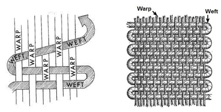
Because yarn thickness, thread count, and fabric weight can differ from one weave to the next, IPC-4412 assigns each distinct combination a style number, such as 106, 1080, or 2116. Figure 2 shows some of these weave styles.
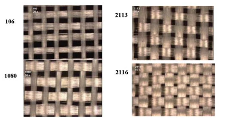
The physical gap between the yarn bundles varies drastically depending on the chosen style. Engineers can select denser glass styles to smooth the dielectric transition across the transmission line, minimizing localized Dk variations and thus skew.
Mechanical Glass Spreading
Traditional glass weaves (like 106 or 1080) feature tightly clustered fiber bundles separated by large resin pockets. To minimize these gaps and mitigate intra-pair skew, laminate manufacturers mechanically flatten the bundles using high-pressure water jets, ultrasonic waves, or mechanical rollers before resin impregnation.
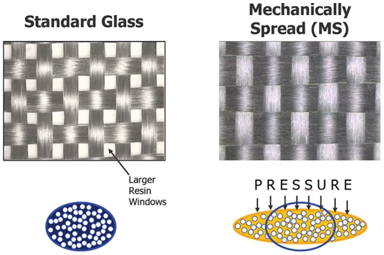
Beyond reducing skew, spread glass also yields cleaner laser-drilled vias because its uniform composition minimizes the resin pockets that cause uneven drilling and plating defects.
Spread glass, however, comes with a challenge. A given spread style, such as 3313, is not fabricated the same way by every manufacturer because no industry standard governs the exact method or quality of mechanical spreading. Figure 4 shows nominal dimensions from two laminate manufacturers, highlighting variations in fiber width due to different levels of mechanical spreading.

This variability means that skew performance can vary drastically from manufacturer to manufacturer. For example, a 14-inch trace using a specific spread style from one manufacturer might exhibit a low skew of 4 ps, while the same glass style from another might produce a skew as poor as 62 ps over that same distance (Knack 2019).
You cannot simply specify "3313 spread glass" on your fabrication notes and assume your high-speed signals are safe. Worse, if your fabricator switches suppliers mid-production to cut costs, your layout could suddenly and unexpectedly fail without a single schematic change. Generic glass style callouts alone are therefore insufficient for skew mitigation; high-speed signal integrity requires explicitly specifying or auditing the laminate manufacturer.
So how does a tight, non-spread weave compare to spread glass? When selecting a laminate, engineers must weigh the structural and cost differences between a tighter traditional weave and a mechanically spread glass. A tighter weave (like 2116) reduces resin pockets by packing in more yarn strands per inch, while spread glass (like 1067 or 3313) flattens and widens those bundles to significantly reduce the gaps. Table 1 compares the two strategies to help you choose the right one for your design.
Comparison Metric | Tighter Weave (e.g., 2116) | Spread Glass (e.g., 1067, 3313) |
Skew Mitigation | Moderate | High |
Data Rate | Generally safe up to 10 Gbps | Preferred above 10 Gbps |
Laser Drill Compatibility | Poor to Fair | Excellent |
Cost | Lower | Premium |
Table 1: Tight weaves vs. spread glass.
Default to a tighter traditional weave if you are working on budget-conscious, standard designs (such as PCIe Gen 3) where trace lengths are short, and laser microvias are not required. Upgrade to spread glass as soon as your design pushes up into ultra-high-speed data rates (such as PCIe Gen 5/6, DDR5/DDR6, or 112G SerDes) or utilizes a high-density interconnect (HDI) stackup that relies on laser-drilled blind and buried microvias. Although glass-spreading significantly reduces the resin-rich gaps, it doesn't eliminate them entirely. The material remains a composite of glass filaments and resin. Therefore, additional mitigation techniques, or a combination of them, may still be required.
Low-Dk Glass
Low-Dk glass (often referred to as L-glass or NE-glass) is one of the most effective material-level solutions to the skew problem. Low-Dk fiberglass formulations reduce the Dk of the glass filaments from about 6.6 to 4.4. By bringing the glass fibers' dielectric constant much closer to that of the resin, the laminate achieves a highly uniform electrical environment. This minimizes propagation velocity mismatches regardless of trace alignment to the weave. Table 2 compares standard E-glass (the conventional, high-Dk material) with NE-glass.

Low-Dk glass offers clear advantages for high-speed designs, especially once data rates climb above 25 Gbps. It reduces skew significantly without resorting to the complex routing techniques discussed later, such as zigzag routing or angle-based methods that increase board area. The trade-offs are cost and availability: low-Dk laminates carry a substantial price premium, and many PCB fabricators don’t stock these specialized glass styles, which can extend lead times. Critically, low-Dk glass is often combined with spread glass; without spreading the bundles, resin-rich gaps remain, limiting the skew-reduction benefit.
Using Dual or Multiple Glass Plies
Using dual or multiple plies of woven glass fabric is a highly effective structural technique for mitigating fiber weave skew in high-speed circuits. Instead of using a single, thick layer of glass cloth to achieve the target dielectric thickness, designers specify two or more thinner laminate layers (e.g., two layers of 106 or 1067 glass instead of one layer of 2116 or 7628). Because the glass yarns in each distinct ply are woven independently, their weave patterns don’t perfectly align when stacked. The result is a more uniform dielectric environment and, in turn, less skew.

The advantage of the multi-ply approach is availability. Most PCB manufacturers support it without requiring specialized or proprietary equipment. However, thinner glass styles and additional handling increase raw material and fabrication expenses. Furthermore, stacking multiple thin plies can introduce slight variations in the final dielectric thickness.
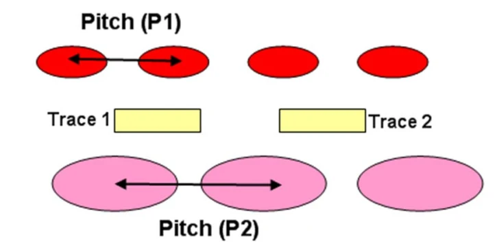
For stripline traces, designers can use two weaves with different pitches for the top and bottom substrates to average out Dk variation (Figure 6).
Having covered what the laminate can do for skew mitigation, we now turn to what the designer can do at the routing stage.
Geometric Alignment: Matching Trace Pitch to Weave Pitch
One fiber-weave skew mitigation technique is to match the pitch of the differential pair's legs to the bundle pitch of the glass fabric. By matching these geometries, both the positive and negative traces are forced to sit on identical regions of the glass-and-resin matrix along a straight path, as illustrated in Figure 7.
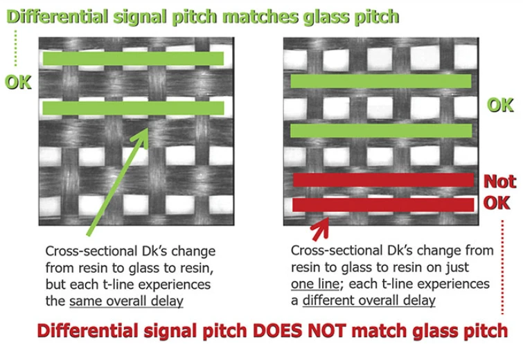
If one trace travels over a dense glass bundle center, its complement travels over an adjacent bundle center; likewise, if one trace crosses a resin-rich region, its complement crosses a similar one, balancing propagation velocity and neutralizing intra-pair skew. To calculate the bundle pitch for a given weave style, you need the fabric count specified in the IPC-4412 standard, which gives the number of yarn bundles per inch in each direction. The bundle pitch is simply the reciprocal of that count. For example, a 1080 fabric features a nominal construction of 60 yarns per inch in the warp direction and 47 yarns per inch in the fill direction. This yields a warp bundle pitch of 1/60 = 0.01666 inch, or 16.66 mils. Therefore, to achieve theoretically zero skew along the warp axis, set the trace spacing to an integer multiple of 16.66 mils.
A rigid, matched pitch cannot be maintained in crowded spaces like BGA breakout fields. However, because fiber-weave skew accumulates proportionally with distance, these short breakout bottlenecks contribute little to the overall phase error. Engineers can therefore route through tight pin fields using compact geometries, and then widen the pair's spacing to a multiple of the glass bundle pitch once the path reaches open board spaces. This strategy allows designers to use wider traces that minimize skin-effect and conductor losses while effectively neutralizing skew over long, high-risk segments of the transmission line.
Trace pitch matching has a few practical limitations and considerations. First, it’s hard to ensure traces remain aligned with the glass bundles because of normal manufacturing tolerances. For example, even a slight rotational offset in the registration between the copper artwork and the laminate can cause a long 15‑inch trace to lose spatial alignment with the underlying bundle pattern. Second, because trace pitch affects differential impedance, pitch matching requires choosing a trace width that satisfies both impedance and skew targets for a given dielectric height. Furthermore, many common weaves are non-square; a 1080 glass style, for example, features asymmetric warp and fill counts (60 × 47 threads per inch), causing the required trace spacing to shift entirely whenever a signal turns a 90-degree corner. Square weaves are therefore preferred, as they maintain consistent spacing in both directions. Non-square weaves require design teams to coordinate with their fabricators to track the board's warp and weft directions across the manufacturing stages. When these constraints and manufacturing dependencies are too prohibitive for a layout, engineers can instead use alternative board-level routing techniques.
Angled Trace Routing
Angled routing is a mitigation technique that involves deliberately routing high-speed traces at a non-zero angle (typically 7-10°) relative to the glass fabric's warp or weft direction, rather than parallel to it.
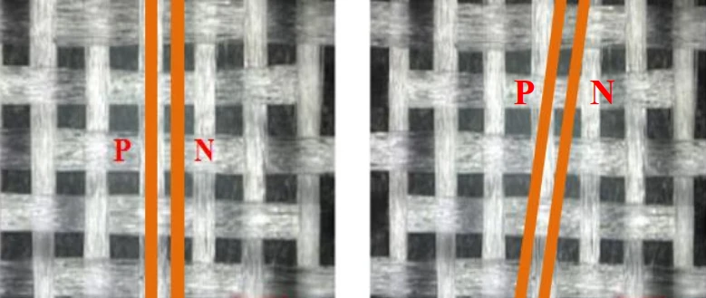
By angling the trace, it crosses multiple glass bundles and resin-rich regions along its length, averaging out the localized dielectric constant variations caused by the weave. This ensures that both traces in a differential pair experience more uniform effective Dk.
A major benefit of angled tracing is its ability to reduce skew on standard glass styles like 1080 or 2116, avoiding the need for premium spread-glass laminates. However, the technique increases board area and adds complexity to trace planning. Component floor planning must be arranged so that routing runs at a specific angle to the glass weave. Additionally, in dense areas, such as BGA breakouts, there may simply not be enough room to route traces off-axis.
While angled routing significantly mitigates differential skew, it introduces a separate signal-integrity penalty: degraded insertion-loss dips caused by glass-weave periodicity. A 2010 DesignCon paper found that a 45° route can produce the lowest-frequency single-cell periodicity resonance (Miller, Blando, and Novak 2010). Angled routing therefore has its own trade-offs for timing skew.
Zigzag Routing
Zigzag routing is a variant of angled routing in which the trace oscillates periodically about its nominal path. Like simple angled routing, its segments run at non-zero angles to the glass weave; what distinguishes it is that the angle alternates direction rather than holding a constant slant. Figure 9 shows a schematic representation of the zigzag routing.
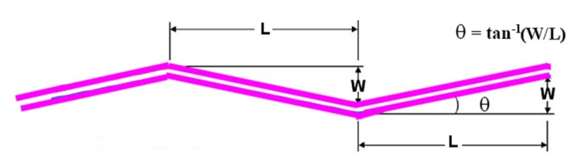
It’s recommended to route the trace such that it traverses at least three times the fiberglass pitch (W ≥ 3 × glass pitch) before reversing direction.
Zigzag routing reduces skew at the cost of board area. Compared with simple angled routing, it can simplify component floor planning by allowing communicating ICs to remain aligned along a standard horizontal or vertical axis, whereas angled routing requires slight placement skew to follow the diagonal trace path. On the downside, zigzag routing introduces physical and electrical penalties that angled routing avoids; because of its turning vertices, a zigzag path can suffer from localized impedance discontinuities, whereas simple angled routing maintains a uniform path with no corners or reflections. Furthermore, the zigzag method results in a longer overall physical length, increasing transmission loss along the channel.
Additional Mitigation Techniques
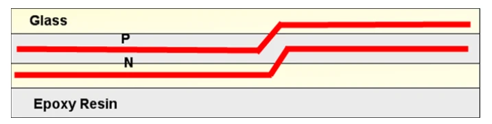
Two additional mitigation techniques exist but are not covered here for the sake of being concise. The first rotates the entire copper pattern relative to the laminate, producing an effect similar to angled routing. The second, sometimes called jogged routing, offsets each conductor by the intra‑pair spacing so the two traces exchange the glass‑rich and resin‑rich regions they originally occupied; this swap of environmental conditions helps equalize their delay (Figure 10).
Conclusion
This article reviewed both material‑level choices and routing‑based strategies for mitigating the fiber‑weave effect. Although a simple, universal remedy would be ideal, most techniques offer only partial solutions whose effectiveness depends on frequency, line length, and the available skew budget. In practice, designers often combine several methods; for data rates above 56 Gb/s—such as 112G PAM4 and PCIe Gen6—NE‑glass with spread‑glass becomes essential, and angled‑routing strategies may still be required to meet tight skew limits.
Related Reading
Part 1: Understanding Fiber Weave Effect: From Glass Weave to Differential Skew
Part 2: Fiber Weave Skew Modeling: Analytical Bounds and Statistical Skew Prediction
Part 3: Fiber Weave Skew Mitigation: Spread Glass, NE‑Glass, and Routing Techniques (this article)
Frequently Asked Questions
How Do You Reduce Fiber Weave Skew?
Fiber weave skew can be reduced through the laminate, the routing, or both. Material-level options include denser glass fabric styles, mechanically spread glass, low-Dk glass such as NE-glass, and dual or multiple glass plies. Routing options include matching the differential pair pitch to the glass bundle pitch, angled routing, zigzag routing, rotating the entire copper pattern relative to the laminate, and jogged routing. Most techniques offer only partial solutions whose effectiveness depends on frequency, line length, and the available skew budget, so designers often combine several. Above 56 Gb/s, NE-glass with spread glass becomes essential, and angled routing may still be needed to meet tight skew limits.
What Is Spread Glass?
Spread glass is woven glass fabric whose yarn bundles the laminate manufacturer flattens before resin impregnation, using high-pressure water jets, ultrasonic waves, or mechanical rollers. Flattening shrinks the resin-rich gaps between bundles, which reduces intra-pair skew and also gives cleaner laser-drilled vias. Spreading does not remove the gaps entirely, because the material is still a composite of glass filaments and resin, so other mitigation techniques may still be needed.
Why Isn't Specifying a Spread Glass Style Enough to Control Skew?
No industry standard governs the exact method or quality of mechanical spreading, so a spread style such as 3313 is not made the same way by every laminate manufacturer. Over a 14-inch trace, a spread style from one manufacturer might show 4 ps of skew while the same style from another shows as much as 62 ps. If a fabricator switches laminate suppliers mid-production, a layout that worked can fail with no schematic change. High-speed designs need the laminate manufacturer specified or audited in addition to the glass style.
Should You Use a Tighter Weave or Spread Glass?
A tighter traditional weave such as 2116 reduces resin pockets by packing in more yarn strands per inch. It offers moderate skew mitigation, is generally safe up to 10 Gbps, and costs less, but its laser drill compatibility is poor to fair. It suits budget-conscious, standard designs such as PCIe Gen 3, where traces are short and laser microvias are not required. Spread glass such as 1067 or 3313 offers high skew mitigation and excellent laser drill compatibility at a premium price. It is preferred above 10 Gbps, for designs such as PCIe Gen 5/6, DDR5/DDR6, or 112G SerDes, and for HDI stackups that rely on laser-drilled blind and buried microvias.
What Is NE-Glass, and How Does It Reduce Skew?
Low-Dk glass, often referred to as L-glass or NE-glass, lowers the dielectric constant of the glass filaments from about 6.6 to 4.4. Bringing the glass Dk closer to the resin Dk makes the laminate electrically more uniform, which reduces propagation velocity mismatch regardless of how the traces align with the weave. Its advantages are clearest once data rates climb above 25 Gbps. The trade-offs are a substantial price premium and limited availability, because many PCB fabricators do not stock these glass styles. Low-Dk glass is often combined with spread glass, because unspread bundles still leave resin-rich gaps.
How Do You Match Differential Pair Pitch to the Glass Weave Pitch?
Set the spacing between the two traces of the pair to an integer multiple of the glass bundle pitch, so both traces sit over equivalent regions of glass and resin along a straight path. The bundle pitch is the reciprocal of the fabric count in IPC-4412. For 1080 glass, with 60 yarns per inch in the warp direction, the warp bundle pitch is 1/60 inch, or 16.66 mils. In BGA breakout fields, where a matched pitch does not fit, route with compact geometry and widen the spacing once the pair reaches open board space; the short breakout segments contribute little to the overall phase error. Pitch matching is sensitive to rotational misregistration between the copper artwork and the laminate, it constrains trace width because pitch also affects differential impedance, and on non-square weaves such as 1080 (60 × 47 threads per inch) the required spacing changes whenever the route turns 90 degrees.
What Angle Should You Use for Angled Routing?
Angled routing typically runs high-speed traces at 7 to 10 degrees to the warp or weft direction of the glass fabric. At that angle, each trace crosses multiple glass bundles and resin-rich regions, which averages the local dielectric constant variations so both traces of a pair see a more uniform effective Dk. It works on standard glass styles such as 1080 or 2116 without premium spread glass, but it uses more board area, requires component floor planning around the routing angle, and may not fit in dense areas such as BGA breakouts. Angled routing can also add insertion-loss dips caused by glass-weave periodicity: a 2010 DesignCon paper found that a 45-degree route can produce the lowest-frequency single-cell periodicity resonance.
How Does Zigzag Routing Compare with Angled Routing?
Zigzag routing alternates the angle of the trace segments around the nominal path instead of holding one constant slant, and the trace should traverse at least three times the fiberglass pitch before reversing direction. Its advantage over angled routing is floor planning: communicating ICs can stay aligned on a standard horizontal or vertical axis. Its costs are localized impedance discontinuities at the turning vertices and a longer physical length, which increases transmission loss. Simple angled routing keeps a uniform path with no corners.
References
Hargin, Bill. 2019a. "How to Avoid Getting Totally Skewed, Part Two." Printed Circuit Design & Fab, July 23, 2019. https://www.pcdandf.com/pcdesign/index.php/current-issue/266-material-matters/13801-pcb-material-matters-1908.
Hargin, Bill. 2019b. "How to Avoid Getting Totally Skewed, Part Three." Printed Circuit Design & Fab, August 21, 2019. https://www.pcdandf.com/pcdesign/index.php/current-issue/266-material-matters/13881-material-matters-1909.
Hargin, Bill. 2019c. "How to Avoid Getting Totally Skewed, Part Four." Printed Circuit Design & Fab, September 20, 2019. https://www.pcdandf.com/pcdesign/index.php/current-issue/266-material-matters/13964-how-to-avoid-getting-totally-skewed-part-four.
Hargin, Bill. 2019d. "What's the Difference between 106 and 1067 Glass?" Printed Circuit Design & Fab, May 22, 2019. https://pcdandf.com/pcdesign/index.php/current-issue/266-material-matters/13668-material-matters-1906.
Intel. 2011. PCB Dielectric Material Selection and Fiber Weave Effect on High-Speed Channel Routing. Application Note AN-528. Intel Corporation. https://www.intel.com/content/www/us/en/content-details/654621/an-528-pcb-dielectric-material-selection-and-fiber-weave-effect-on-high-speed-channel-routing.html.
Knack, Kella. 2019. "The Impact of Glass Weave Styles on Blind Vias and Differential Skew." Altium Resources, September 22, 2019. https://resources.altium.com/p/impact-glass-weave-styles-blind-vias-and-differential-skew.
Miller, Jason R., Gustavo Blando, and Istvan Novak. 2010. "Additional Trace Losses due to Glass-Weave Periodic Loading." Paper presented at DesignCon, Santa Clara, CA, February 2010. https://www.signalintegrityjournal.com/ext/resources/White-papers-App-notes/4119_DC10_Glass_Weave_Losses_SUN_v11.pdf
Nalla, Kartheek. 2016. "Mitigation of Glass Weave Skew Using a Combination of Low DK Spread Glass, Multi-Ply Dielectric and Routing Direction." Master's thesis, Missouri University of Science and Technology. https://scholarsmine.mst.edu/masters_theses/7859.
About the Reviewer

Bill Hargin
,
Founder of Z-zero
Bill Hargin is the founder of Z-zero, the Scottsdale, Arizona, developer of Z-planner Enterprise software for PCB stackup design and material selection. He has more than 25 years of experience in PCB signal integrity and manufacturing, including director-level marketing roles for Mentor Graphics’ HyperLynx software and Nan Ya Plastics’ PCB laminate division. He wrote the book Stackups: The Design within the Design and co-authored DesignCon research on glass-weave skew with Eric Bogatin.