








Read the Full Series
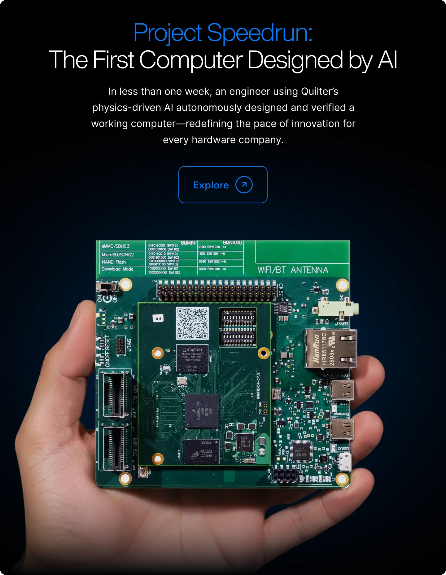
This article is one part of a walkthrough detailing how we recreated an NXP i.MX 8M Mini–based computer using Quilter’s physics-driven layout automation.
On our customer calls we like to ask engineers how they judge the quality of a layout. The answers vary more than you'd expect, but one thing that gets frequently brought up: "Quality is passing DFM on the first go."
By that definition, this article is an accounting of how Project Speedrun scored. The lessons learned can be applied to any board, routed by a human or AI.
Project Speedrun recreated an NXP i.MX 8M Mini computer with Quilter's physics-driven layout automation, documented across five parts: preparing the design, compiling it into a layout, cleaning it up for production, validating it under real workloads, and building its firmware. What the series skipped is everything that happened between "the layout is done" and the unboxing assembled boards in our lab: the quotes, the CAM review, the 58 findings Sierra Circuits raised against our data, and the back-and-forth that resolved them.
Can an AI-Designed PCB Be Manufactured?
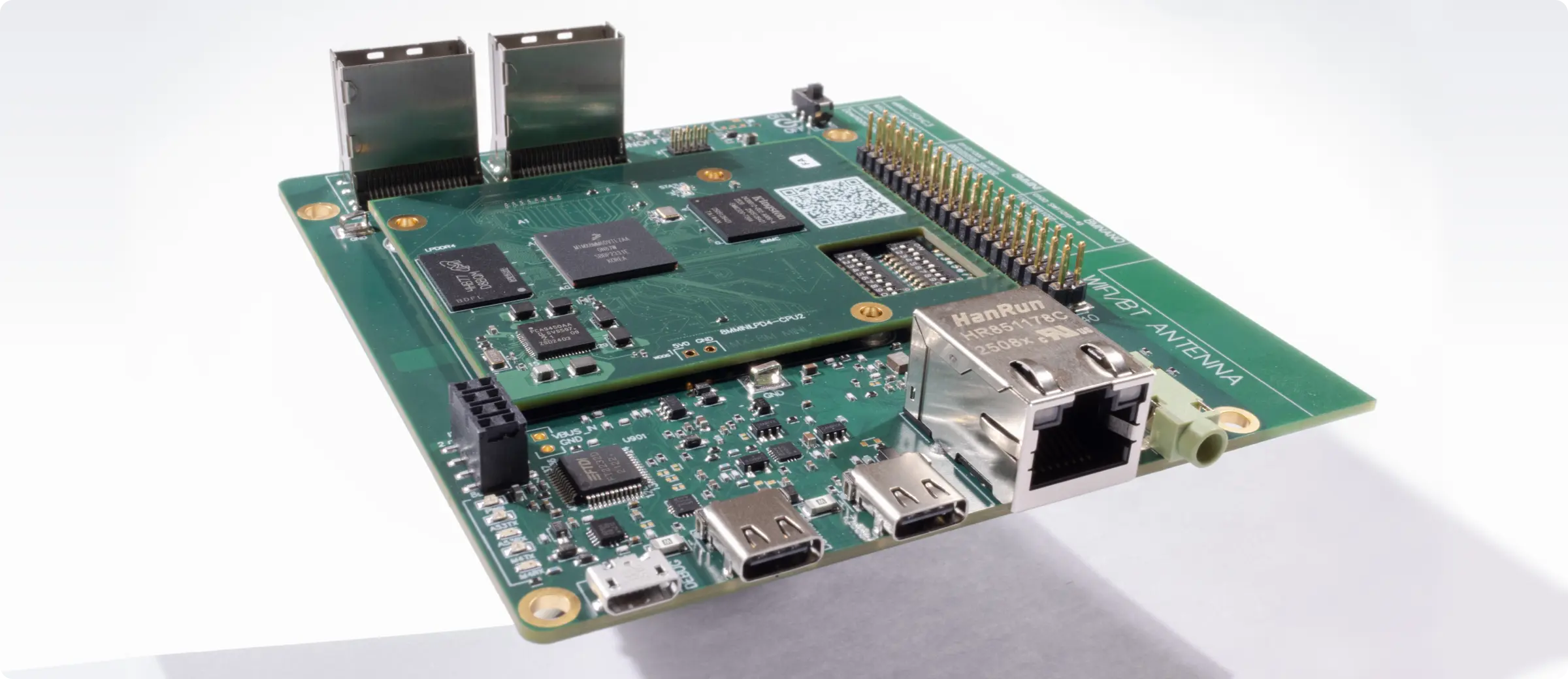
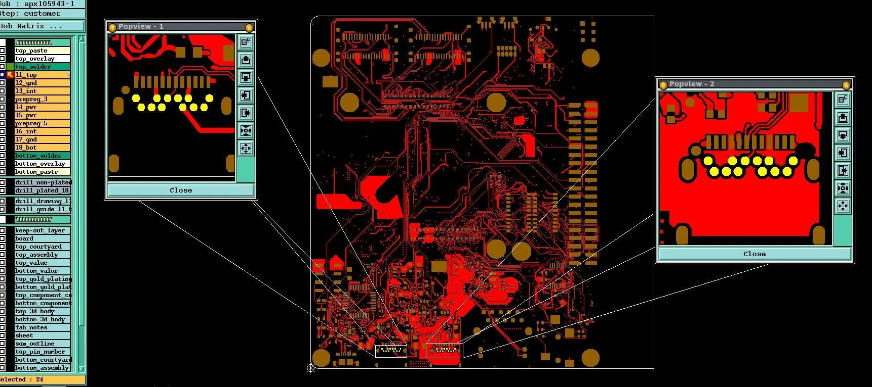
Let’s address the elephant in the room first. Yes, PCBs designed with AI assistance are manufacturable if the AI tools are used correctly. Sierra built 10 SOMs and 10 baseboards, and every single pair powered up and ran. One has now been running Linux on Ben's desk for three months straight without a reboot.
A more interesting question is what a serious fab's engineers find when they comb through an AI-assisted design with the same tools and the same skepticism they apply to everything else. The answer: 58 findings across the two boards. A "finding" is a question the reviewer raises, not necessarily a defect. Of those, 48 were documentation gaps, library errors, BOM inconsistencies, and supply-chain substitutions, the same items that can surface on any board, however it was routed. Only 10 touched the physical design, and most of those turned out to be a miscommunication about which manufacturing process we'd been quoted for, not a problem with the layout.
Project at a Glance
Boards | SOM plus carrier baseboard |
Layers | 8 per board |
Total review findings | 58 |
Baseboard issues | 37 |
SOM issues | 21 |
Minimum geometry | 2.2 mil trace and space |
Fine-pitch process | mSAP, LDI, and laser-filled blind vias |
The Two Boards
System-on-Module Specifications
The SOM (QSOM-IMX8-98.7) carries the processor. It's an 8-layer, controlled-impedance board with 2 mil trace and space, laser-drilled and filled vias, and DDR4L memory at 2133 MHz, built on Ventec VT-47 high-speed laminate, 48 mils thick, with an ENIG (electroless nickel immersion gold) finish.
Baseboard Specifications
The baseboard (NXP_8MMINI-BB) is the carrier the SOM plugs into. It's also 8 layers, 62 mils thick, at 3 mil outer and 3.25 mil inner trace and space, with 50 ohm single-ended and 100 ohm differential impedance targets and a mixed through-hole and surface-mount assembly. Sierra raised 37 findings on it, all resolved before manufacturing.
Both boards were built to IPC-6012F Class 2, the acceptance class for dedicated-service electronics, and assembled to IPC-A-610 Class 2.
What the 58 DFM and DFA Findings Actually Were
Sierra's handbook defines DFM as "the manufacturer's opinion on the manufacturability of products” and a properly-executed DFM as “an amalgamation of all the stakeholders including designers, engineers, contract manufacturers, and material suppliers.” DFM ensures that “the design is optimized and does not have unnecessary cost embedded in it.”
DFA, design for assembly, asks the same question about the assembly of the board: whether the components on the BOM can be placed and soldered onto it as documented.
Both DFM and DFA reviews happen in CAM, the computer-aided manufacturing step where the fab converts your design files into machine programs, and where a human reviewer reads your data the way the factory will.
Category | Findings | Share | What It Covers |
DFM Capability | 10 | 17% | Design pushed beyond the standard, low-cost process |
DFM Documentation | 18 | 31% | Missing or unclear fab specifications |
DFA Assembly | 17 | 29% | Footprints, polarity, pin numbering |
DFA Supply Chain | 13 | 22% | BOM errors, alternates, consigned parts |
Why Published Manufacturing Capabilities Can Differ From DFM Defaults
Here are a few direct quotes from Sierra’s DFM report on the SOM: "Outer and inner trace/space is 2mil, please fix it minimum 3mil or more" and "Drill to copper spacing is 3.5mil, please fix it minimum 7mil or more."
These findings were surprising to us at first, because we had scrutinized Sierra's capabilities page before Ben began working on the layout, and both boards were quoted under their Micro tier, which uses mSAP and LDI.
Parameter | Standard | Advanced | Micro |
Min Trace / Space | 4 mil | 3 mil | 2 mil |
Smallest Laser Drill | 5 mil | 4 mil | 4 mil |
Min Finished Hole | 4 mil | 2 mil | 2 mil |
Process Pad | D + 12 mil | D + 4 mil | D + 4 mil |
Impedance Tolerance | ±10% | ±5% | ±5% |
Max Aspect Ratio | 10:1 | 10:1 | > 20:1 |
Min Dielectric | 4 mil | 3 mil | 2 mil |
Source: Sierra Circuits rigid and HDI PCB capabilities. The Micro tier requires mSAP and LDI.
The Micro tier does deliver what it promises, but a fab's standard DFM review doesn't automatically apply Micro-tier rules to an incoming design. The checks run uniformly against the conservative, standard process. So a board quoted for 2 mil trace and space gets flagged the moment it drops below 3 mil.
Published (Micro Tier) | What DFM Flagged in Practice |
2 mil trace and space | Anything below 3 mil trace/space |
4 mil laser drill | 7 mil drill-to-copper required |
D + 4 mil process pad | 15 mil pads requested for 5.9 mil holes |
Plated-shut blind vias | Semi-additive process questioned |
±5% impedance tolerance | Impedance relaxed to ±20 to 30% |
None of these were due to design issues. They were the quoting team and the DFM engineering team not sharing the same picture of which process the board was built for, and us not communicating all of this proactively enough. Every single one was resolved once we confirmed the tier directly with Sierra's engineers. One big lesson learned here is that you should engage the fab's engineering team before you order to confirm the process tier and pre-approve the design rules that apply.
Understanding the Manufacturing Processes Behind the Constraints
For a drilled hole to land where intended, several things have to go right. The drill bit can wander up to ±2 mils on a mechanical drill. The copper layers themselves shift, because laminate shrinks and moves under lamination heat and pressure, and layer-to-layer registration is only guaranteed to be about 2 mils. And the finished hole comes out up to 3 mils larger or smaller than drawn, because plating thickness depends on the copper around the hole. Worst case, that's 2 + 2 + 1.5 mils of error against a hole that’s supposed to be 3.5 mils away from copper. On a bad day, the hole lands on the copper. Sierra's data on drill breakout states that at 2 mils of clearance the probability of breakout is about 98%. At 6 to 7 mils it's essentially zero.
That is why those findings were resolved once the process tier was confirmed. The Micro tier uses different machines. Laser drills don't wander the way mechanical ones do, and Sierra's vision drilling systems X-ray the internal layers after lamination, measure how much the material moved, and rescale the drill program to match.
How mSAP and Laser-Filled Microvias Enabled BGA Fanout
The i.MX 8M Mini uses a 0.5 mm pitch BGA with 196 balls. Pad-to-pad centers sit 19.7 mils apart. With 10 mil pads, that leaves a 9.7 mil routing channel to escape a signal between two balls. To fit one trace, you need a trace plus two spaces. At a 3 mil minimum you'd need 9 mils (3 + 3 + 3), which only just fits. Going down to 2.2 mil trace widths added breathing room for BGA escape routing which resulted in higher routing completion along with room for delay tuning on the DDR4 bus. Sierra's DFM flagged the <3 mil trace and space and, as a direct consequence, the 3.5 mil drill-to-copper spacing that fine geometry forces inside the BGA field.
Understanding what it takes to produce a board with 2 mil traces can guide you on which fabs can manufacture your board at all. Conventional traces are made subtractively: start with a sheet of copper, etch away everything that isn't a trace. The etch bath works sideways as well as down, undercutting the resist and leaving a trapezoidal cross-section, and the resulting width is controllable to about 0.5 mil. On a 6 mil trace that's an acceptable margin. On a 2 mil trace it's a 25% error, enough to exceed impedance tolerances and severely reduce yield.
Therefore, standard subtractive etching can not reliably produce boards with 2 mil traces. This is where mSAP available on the Micro tier comes in. mSAP, the modified semi-additive process, is a PCB fabrication method that builds traces additively. Instead of etching copper away, it plates copper up onto a thin seed layer only where the lithography defines a trace. Because the trace geometry is defined by imaging rather than by etch chemistry, sidewalls come out near vertical and width control tightens to about 0.1 mil.
Vias also had to get special treatment. With standard blind micro-via build-up construction, the outer transitions (ie. L1 to L2 and L7 to L8) are laser-drilled at 4.5 mils and filled with copper and plated shut. This fans out BGAs and other fine-pitch components to the first inner layer without spending the routing channel on big mechanical pads. Then core layers (ie. L2 to L7) are conventionally drilled and plated. Since our design used only through-vias, Sierra requested to use stacked laser-drilled construction (all transitions are laser-drilled), which enabled the tighter drill-to-copper while keeping registration allowance. The only down-side for us was the added lamination and drilling cycles that resulted in longer fabrication time.
Controlled-Impedance Tradeoffs in the Final Stackup
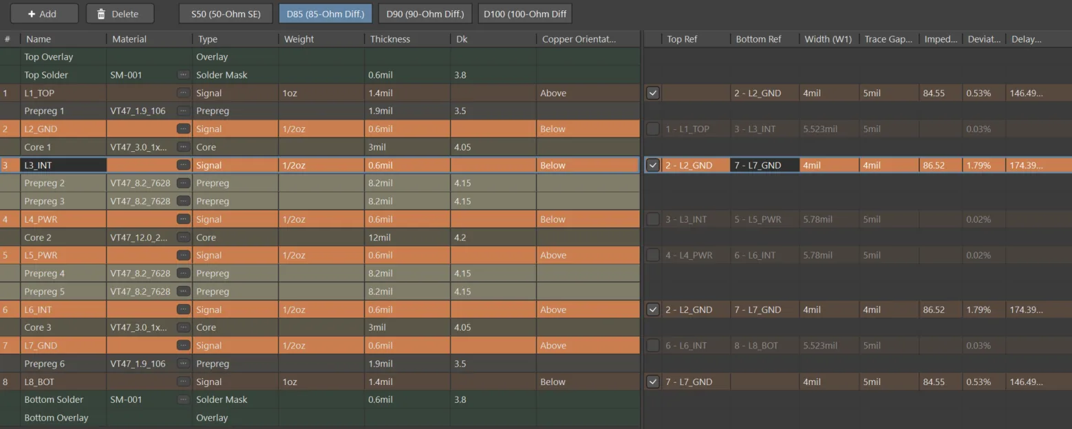
Two findings in Sierra's review would look alarming out of context. The SOM's 50 ohm single-ended target on the outer layers came back as 62 ohms, approved at ±30%. The baseboard's 100 ohm differential target came back as 92 ohms, approved at ±20%. In both cases the achievable geometry on the outer layers, given everything else the stackup had to satisfy, didn't hit the nominal number.
First, the term itself: controlled impedance means the fab guarantees that designated traces hit a target characteristic impedance within a stated tolerance, verified on test coupons fabricated on the same panel as your boards. Impedance discontinuities reflect signal energy, which is why every high-speed interface on these boards specifies a target.
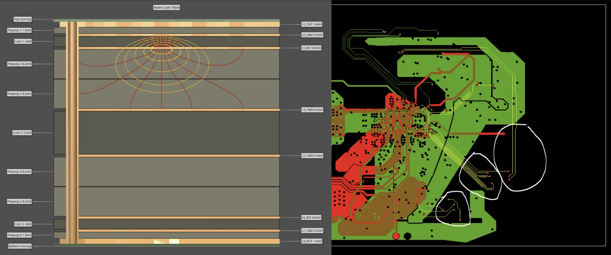
Here's why these values were acceptable. Outer layers are the worst place on a board to control impedance. An outer trace is a microstrip with a dielectric below and solder mask of unpredictable thickness and Dk above. An inner stripline sits between two reference planes in homogeneous material, which is why fabs will hold ±5% there and hedge on the outer layers. Because the outer layers also get plated, their final copper thickness depends on the drilling strategy, which on this board meant that 1.2 to 1.4 mil variation we'd already accepted. Everything that mattered electrically, the DDR4L interface above all, is tolerant far beyond 5% because it is intended to be produced with low-cost consumer-grade materials - what matters much more is the delay tuning of the interface signals and reference plane coupling for SI. The differential interfaces (PCIe, MIPI, etc.) came within the target tolerances.
The lesson learned here is that impedances may vary GREATLY between your solver-determined trace width and what the fab calculates based on their processes and internal changes to your layer stack.
There was a stackup lesson hiding here too. You can build a beautiful, precise layer stack in your EDA tool from the laminate datasheets, and it will still be wrong, because datasheets don't tell you how much prepreg squeezes out during lamination. Establish the real stackup with the fab before you start routing. In our case that conversation revealed one more issue. The TU-768 laminate used by NXP’s reference design wasn't available in the domestic supply chain, and the stackup was rebuilt around Ventec VT-47 while holding the impedance targets. Even the dielectric is a supply-chain item and that needs to be accounted for.
The Unglamorous Majority: Assembly and Supply Chain Findings
The largest share of issues, 30 of 58, came from assembly and supply chain. None of these were unique to Project Speedrun or caused by the fact that the board was laid out with AI assistance. These issues are typical and can occur with any board. A fast automated layout doesn't remove the need to validate every footprint, every BOM line, and every part substitution, nor can it resolve supply chain shortages.
Footprint, Pin-Numbering, and Polarity Findings
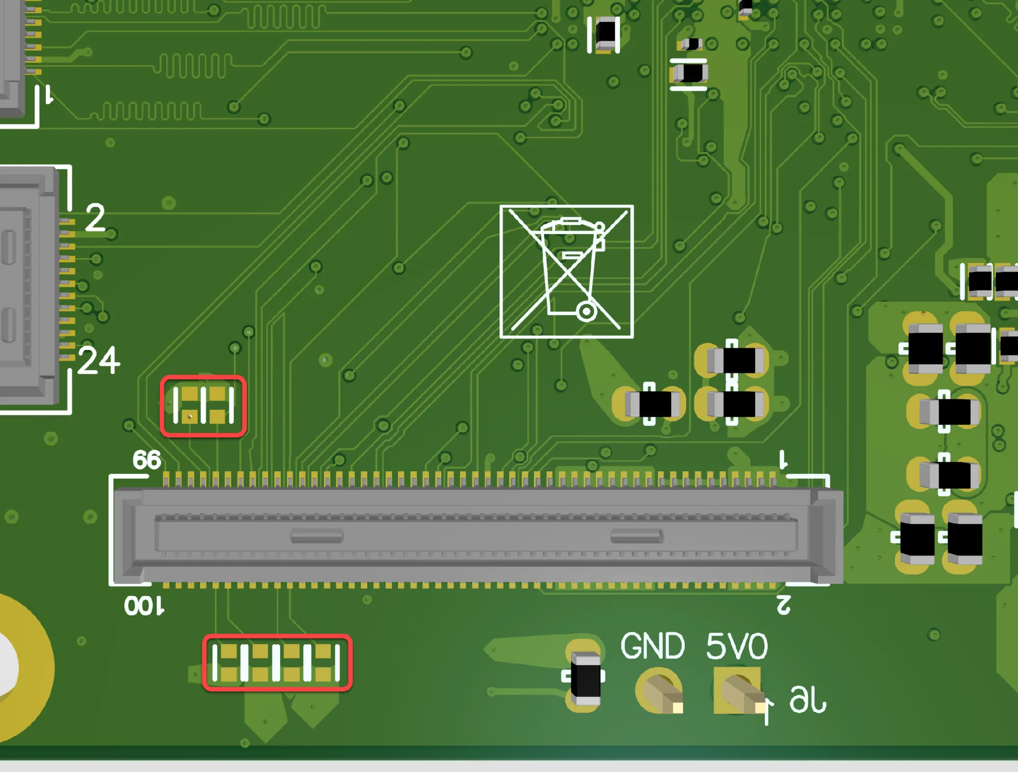
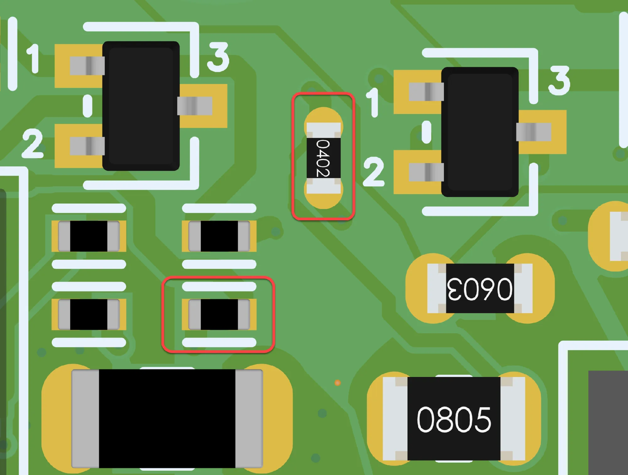
The same manufacturer part number appeared on the baseboard with two different footprints, created for hand-solderable 0 ohm jumper options. Three land patterns didn't match their component datasheets. Six pin-1 and polarity marks on the assembly layers were ambiguous to DFA engineers. One connector had optional 0.1 inch alignment pegs (a part number variant) on a 0.062 inch board, which means the pegs poke out the far side directly into the connector mounted opposite (that option was NOT used in the BOM, though DFA checks automatically flagged it as an issue based on the footprint).
BOM and Alternate-Component Findings
Three resistor description-to-MPN mismatches showed up on the SOM, where auto-generated descriptions didn't match the specified part numbers. Alternate-part suggestions needed a full-spec review. This was ultimately caused by attempting to tell the fab to use generic R/C chip components already loaded into their assembly lines. Assemblers seem increasingly to demand explicit orderable MPNs even for “jelly bean” parts these days. One suggested inductor alternate was rejected for the wrong current rating and package size before an acceptable one was approved.
Supply-Chain and Consigned-Part Findings
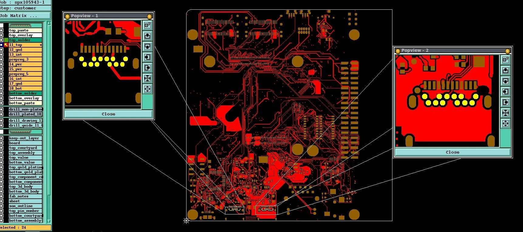
The supply chain drove 13 findings. The Ethernet jack, the PHY, the DDR4L, and the eMMC all had to be consigned, meaning we sourced the parts ourselves and shipped them to Sierra rather than having the fab buy them. The original USB-C connector went out of stock, and its replacement had a different footprint. The footprint downloaded from the vendor's library service was riddled with errors, including plated through-hole pads tented over with solder mask. Tenting, covering a hole completely with solder mask, can be a legitimate choice for vias you want sealed. On a pad that has to take solder, it's a defect twice over. First, the mask itself blocks the joint from forming at all. Second, these pads were through-holes, the sealed barrels could trap plating chemistry that would bleed out in the reflow oven and contaminate the joints around them. Sierra flagged it and fixed the mask and paste openings in CAM, and the library got corrected at the source.
31% of the Issues Were Just Documentation
The most preventable category was documentation; 18 of the 58 issues, 31% of the total, came from an imperfect data package.
The “data package” in this case mainly consisted of fabrication drawing and notes layers in the PCB outputs, derived from the original NXP EVK design files, and as such had to be updated to reflect the new design by Quilter. In light of the following, it is debatable whether modifying an existing set of fab drawings and notes for a new layout actually saves time versus building them from scratch. Fabrication notes inherited from the forked NXP reference design were somewhat stale.
The baseboard's impedance tables contradicted the layout data in three places. The intent behind certain solder mask and paste decisions, like paste deliberately omitted from do-not-install pads, wasn't documented.
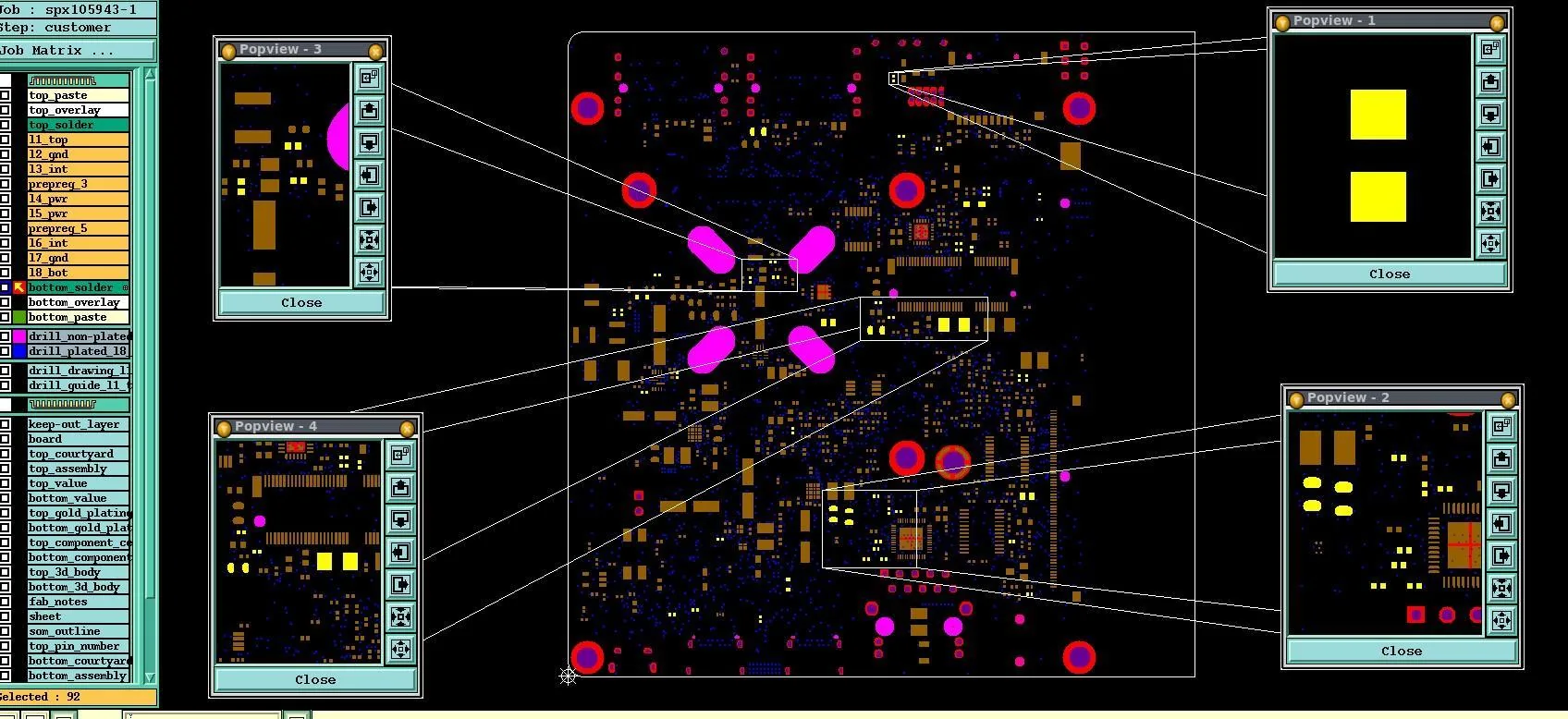
In Ben’s own words “a lot of that was on us for not being quite diligent enough with every single detail up front." No matter how good the layout is, the designer has to hand-assemble the documents describing it: fab drawings, drill charts, stackup table, impedance callouts, IPC class, netlist. Nearly a third of all friction on this project came from hand-maintained documents drifting out of sync with machine-generated data. Including superfluous detail in fab and assembly notes often leads to additional delays while the CAM team seeks clarification on meaning or flags what appear to be conflicting requirements.
A related question came up on reference planes. A few traces were flagged as possible impedance deviations when inspected in 2D by the CAM team, even though the stackup had already accounted for them, because power pours weren't used as reference returns for the impedance-controlled traces. The original NXP evaluation board hit the same flag on an earlier test run. It raises a fair industry question: do the ODB++ and IPC-2581 formats need richer impedance-profile data so a fab's CAM DFM tools can resolve this automatically instead of raising it by hand?
Lessons Learned and What We’d Do Differently
Manufacturing the Project Speedrun boards was no different from building any other fine-pitch, controlled-impedance board. Here are generalized lessons that can be useful to engineers working on a PCB of any kind.
- Engage the fab's engineering team before ordering. Confirm the process tier in writing and pre-approve the rules that depend on it.
- Get the real stackup from the fab first. Datasheet dielectrics don't survive lamination unchanged, and your laminate might not survive the supply chain either.
- Triple-check the data package. Generate fab notes, IPC specs, and impedance profiles from the EDA output so they're complete and consistent every time.
- Validate libraries and BOMs against datasheets. Cross-check every land pattern, pin-1 mark, and part number against the real component. Where possible, REDUCE the complexity of footprints in your library and enforce common normalized assembly layers.
- Budget impedance margin during design. Expect ±20 to 30% on outer layers, and route the signals that can't tolerate it on inner layers.
Conclusion
The most important lesson from this chapter is that the knowledge that resolved all the DFM and DFA issues for the most part isn't written down anywhere. A designer learns what a fab will flag over 1, 5, 20 years of working with them, watching which boards fail and why.
We proved that a board designed with AI assistance can be manufactured. In fact, the AI-generated layout added no manufacturing friction that a hand-routed board wouldn't have. The friction that did occur came from the manual parts of the process: validating footprints, keeping BOM data clean, writing fab notes, and resolving miscommunications with the fabricator. Engineers at every company we talk to still do all of that work on every board. And it is often the work that is not visible from the first look at the hardware project schedule, the work that consumes a lot of time but ultimately ensures the project’s success.
Quilter can speed up the board layout process, but it does not replace decades of experience and design intuition that goes into producing working hardware.
Frequently Asked Questions
Can an AI-designed PCB be manufactured at a production fab?
Yes. Project Speedrun's AI-generated i.MX 8M Mini boards were fabricated and assembled at Sierra Circuits on an 8-layer, controlled-impedance stackup with 2 mil trace and space and laser-drilled vias. Of the 58 issues raised during manufacturing review, the large majority came from documentation, libraries, BOM, and supply chain, not from the routing.
What are laser-drilled and filled vias, and why use them?
They are small blind vias formed by laser rather than mechanical drill, then plated shut with copper. On the SOM they connect the BGA pads to the first inner layer without consuming the routing channel that a large mechanically drilled pad would. Combined with mechanical through-holes through the board core, this hybrid drilling approach is what makes fine-pitch, 2 mil boards practical to build at volume.
What is mSAP?
The modified semi-additive process (mSAP) builds up copper traces additively rather than etching them from a full copper layer. It supports the fine 2 mil geometry the SOM required, and it is part of Sierra's Micro manufacturing tier along with laser direct imaging.
Were the manufacturing issues caused by Quilter's layout quality?
No. Of the 58 issues, 48 were documentation, assembly, or supply chain items that exist on any complex board. The remaining capability issues were mostly about confirming which process tier the board was quoted under, plus honest impedance-tolerance and drill-spacing tradeoffs inherent to a fine-pitch design.
What is the most common source of DFM and DFA issues?
On these boards, documentation gaps were the single largest category at 31%, followed closely by assembly issues like footprint, pin-numbering, and polarity ambiguities. Both are preventable with automated fab-note generation and systematic library and BOM validation.
Sources
Sierra Circuits. The Designer's Handbook for DFM. Sunnyvale, CA: Sierra Circuits Inc., January 2024.
Sierra Circuits. "Rigid PCB Capabilities." Accessed August 5, 2026. https://www.protoexpress.com/products/rigid-pcb/.
Sierra Circuits. "Making Sub 3/3 a Reality." Sierra Circuits Blog. https://www.protoexpress.com/blog/making-3-mil-a-reality/.
Sierra Circuits. "Annular Rings Explained by a PCB Manufacturer." Sierra Circuits Blog. https://www.protoexpress.com/blog/dont-let-annular-rings-drive-you-crazy/.
Sierra Circuits. "Difference Between Microstrip and Stripline." Sierra Circuits Blog. https://www.protoexpress.com/blog/difference-between-microstrip-stripline-pcb/.
Sierra Circuits. "PCB DFM Tool (Better DFM)." Accessed August 5, 2026. https://www.protoexpress.com/tools/pcb-dfm-tool/.
Authors: Amit Bahl, Ben Jordan, Iryna Zhuravel
.webp)




.webp)