







Read the Full Series
This article is one part of a walkthrough detailing how we recreated an NXP i.MX 8M Mini–based computer using Quilter’s physics-driven layout automation.
The fiber weave skew or effect is the timing mismatch that appears when the two traces of a differential pair travel over different mixtures of glass and resin inside a PCB laminate. Glass bundles have roughly twice the dielectric constant of the surrounding resin, near 6 versus near 3, so a signal over glass propagates measurably slower than one over resin. The resulting intra-pair skew accumulates with trace length, closes the receiver’s eye diagram, and produces sharp resonance nulls in the SDD21 insertion loss response.
Although the fiber-weave effect is well documented, existing literature can be dense or difficult to digest. This article series offers a more approachable, intuitive breakdown to help engineers fully grasp the underlying principles. As the first installment of a three-part series, this article begins with PCB laminate construction to explain how dielectric variations between fiberglass bundles and resin-rich areas cause localized velocity mismatches, leading to intra-pair timing skew in differential signaling. It then shows how this phenomenon drives eye-diagram closure and creates characteristic resonance dips in the line’s frequency response, laying the foundation for the more advanced discussions including the mitigation strategies in the upcoming installments.
Understanding the Laminate Construction
To understand how a printed circuit board interacts with high-speed digital signals, it’s important to look past its smooth exterior to its internal material anatomy.
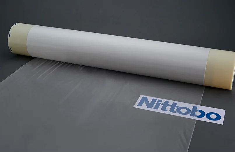
PCB laminate construction depends on three specialized manufacturing stages. First, industrial textile companies like Nittobo produce fiberglass yarns and weave them into continuous rolls of highly uniform fabric — woven exactly like your favorite pair of jeans, but with glass bundles instead of cotton.
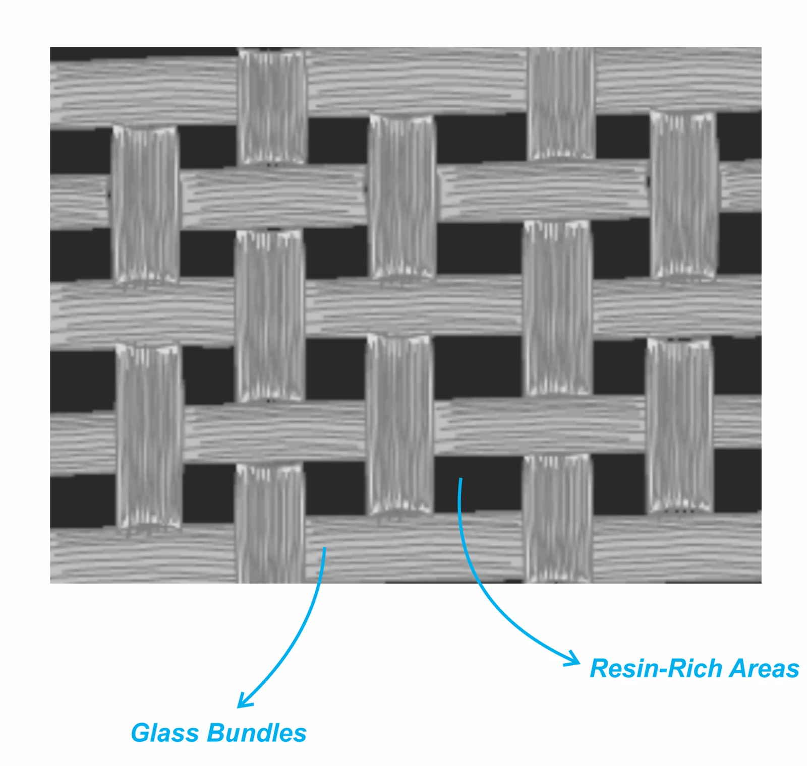
Next, companies such as Isola Group and Rogers Corporation impregnate woven fiberglass with proprietary resin systems. The resin-encased fiberglass weave becomes two products: Prepreg, which is partially cured to remain soft and flexible, serving as a bonding agent between PCB layers; and Core, which is fully cured into a rigid sheet with thin copper foil bonded to one or both sides. Figure 2 details the arrangement of woven glass yarn and resin in a standard PCB laminate layer.
The third tier in the supply chain is the PCB fabricator which purchases off-the-shelf laminate materials and stacks them according to the engineer’s design files.
While the glass cloth provides high mechanical strength, dimensional stability, and excellent thermal resistance, the resin serves as the primary bonding layer that fuses the composite layers together. Equally important, the resin establishes a dielectric barrier between copper sheets.
The Physics of Laminates: Non-Uniform Dielectrics
As a composite material consisting of alternating glass-rich and resin-rich regions, a standard PCB laminate forms a non-uniform medium for electrical signal transmission in which the propagation velocity fluctuates with every change in the underlying material. To unpack this phenomenon, we need to review the fundamental factors that govern the propagation velocity of an electromagnetic wave. By applying Maxwell’s equations to time-varying electromagnetic fields, it can be shown that the propagation velocity of a wave through any medium is governed by the relation:
\[v = \frac{c}{\sqrt{\varepsilon_r \cdot \mu_r}}\]
Equation 1
where c is the speed of light in a vacuum (approximately 3×10⁸ m/s), εr is the relative permittivity, and μr is the relative permeability of the material. In plain terms, relative permittivity εr describes how easily a medium’s molecules polarize in response to an electric field, while relative permeability μr describes how readily they align with a magnetic field. Physically, forcing a medium’s molecules to repeatedly polarize in response to the shifting electric field and align with the shifting magnetic field takes finite time and energy. Consequently, electromagnetic wave propagation slows down in environments with high εr and μr, explaining why these parameters appear in the denominator of Equation 1.
Because PCB substrates are entirely non-magnetic, their relative permeability is approximately equal to that of a vacuum (μr≈1). Consequently, for practical hardware design, Equation 1 simplifies to rely solely on the material’s relative permittivity εr. In the electronics and PCB industry, this specific parameter is more commonly referred to as the dielectric constant denoted by Dk. Therefore, the signal propagation velocity can be expressed as:
\[v = \frac{c}{\sqrt{D_k}}\]
Equation 2
The dense glass bundles possess a high dielectric constant Dk≈6, while the resin-rich windows filling the gaps possess a lower dielectric constant Dk≈3. Because the glass bundles have roughly double the dielectric constant of the epoxy resin, an electromagnetic wave traveling through a glass-rich region moves at a significantly lower velocity than a signal propagating over a resin-rich path. Consequently, signals traveling along identical trace lengths on the same board will experience different propagation velocities depending on the underlying glass-resin pattern. The worst-case scenario is depicted in Figure 3.
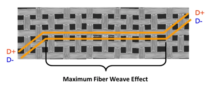
In this case, one trace runs atop a glass bundle and the other over resin-rich windows, establishing the lower and upper bounds for signal propagation velocity. Traces that traverse a combination of glass-rich and resin-rich regions will experience an effective velocity between these two extremes. This material-induced timing variation is called the fiber-weave effect.
How the Fiber Weave Effect Creates Differential Timing Skew
The glass weave structure introduces local velocity variations that drive timing skew in differential pairs. Optimal differential transmission requires the complementary signals to arrive at the receiver simultaneously. When the glass weave effect forces the lines to experience different velocities, one signal outpaces the other, breaking their symmetry and generating intra-pair skew. Figure 4 conceptually illustrates differential signal propagation, assuming an environment in which the lower trace has a lower propagation velocity than the upper trace.
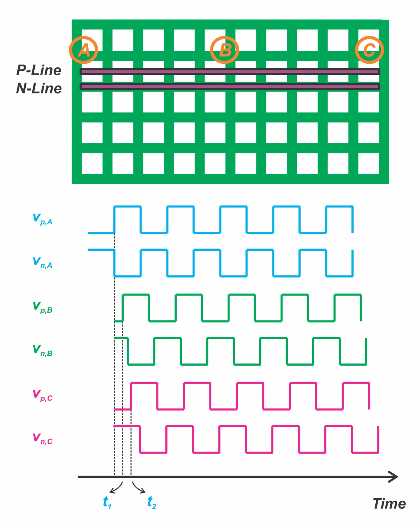
The differential signals originate at Point A in perfect alignment, where the positive and negative waveforms (vp,A and vn,A) are identical but inverted. As they propagate, local material variations delay the negative line relative to the positive line, leading to timing skew at point B (vp,B and vn,B). The skew accumulates over distance, making the timing separation between the positive and negative lines even greater at point C (vp,C and vn,C). If the trace length is long enough, the cumulative skew will completely degrade the signal, preventing the receiver from properly reconstructing the data. As detailed in the following section, this timing skew directly degrades the receiver’s eye diagram and leads to notch-filter-like behavior in the frequency domain.
Eye Diagram Degradation Due to Fiber-Weave Skew
The impact of timing skew on transmitted signal quality is best illustrated by exploring how misalignment between differential signals compromises the receiver’s sampling margin. To analyze this behavior, MATLAB simulations are utilized to model an otherwise ideal differential pair where the complementary negative signal is delayed relative to the positive signal. Figure 5 displays the simulated 10-bit random data stream modeled both with and without timing skew.
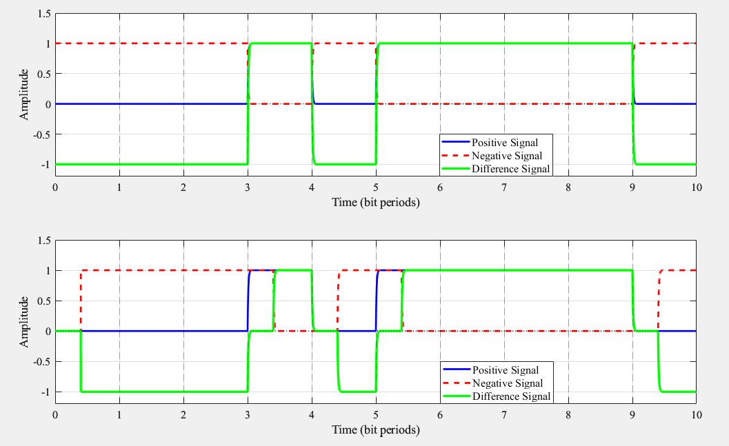
Across both subplots, the positive signal is blue, the negative is red, and the difference signal is green. The upper subplot shows the ideal case with zero timing skew, whereas the lower subplot introduces a propagation delay on the negative line equal to 40% of the bit period.
In the ideal case, the differential output switches cleanly between +1 V and -1 V because the aligned complementary lines transition simultaneously. However, with the skew introduced in the lower subplot, the difference signal occasionally drops to and plateaus at 0 V. This phenomenon occurs after every transition in the input data stream. Because the negative signal lags behind the positive one, the receiver experiences a temporary state where both lines dwell at the same voltage level before the delayed edge finally arrives, introducing an invalid 0 V logic state.
This is an important observation, and to truly understand its significance, we must evaluate the waveform from the perspective of the receiver. Under normal operating conditions, the receiver reconstructs the transmitted data by sampling the difference signal, expecting to see clear, decisive logic levels of +1 V or -1 V. However, in the skewed case, the difference signal occasionally lingers at 0 V, leaving the receiver unable to determine whether a logical high or low was intended.
For example, observe the behavior in the lower subplot of Figure 5 during the time period between t=3 and t=4 bit periods. This window immediately follows a data transition, causing the difference signal to drop to 0 V and dwell there for exactly the duration of the skew — equal to 40% of the bit period. Throughout this 0.4 bit-period interval, the receiver is left in an indeterminate state and cannot correctly determine the transmitted data. In this example, the receiver has a valid sampling window of only 0.6 bit-periods to correctly detect and process the incoming data.
How can we ensure we have identified the absolute worst-case scenario for the receiver’s sampling window? While analyzing a single bit period provides valuable insight, it only captures one specific logic transition. In practice, a digital system processes millions of random bit patterns, meaning engineers must evaluate all possible combinations to guarantee that a worse or unexpected edge case has not been overlooked. To achieve this comprehensive view, we turn to the eye diagram.
By slicing the continuous waveform into overlapping two-bit intervals and overlaying them on top of one another, the eye diagram acts as a composite visual summary. The eye diagram allows us to monitor every possible transition simultaneously, exposing the maximum reduction in both horizontal and vertical sampling margins. To visualize this behavior statistically, a long 1000-bit data stream is generated to construct the eye diagrams displayed in Figure 6.
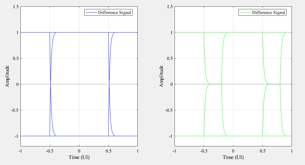
While the unskewed case on the left displays a wide eye diagram with a horizontal width of about 1 bit period, the skewed case on the right reveals a heavily constricted opening with an eye width of only about 0.6 bit-periods, where the finite rise and fall times of the signal transitions account for the slight further reduction in both margins.
The Impact of Timing Skew on SDD21 Resonance Dips
The fiber-weave effect has a profound impact on the frequency response of a differential path as well. To better visualize how this timing skew alters frequency-domain behavior, it is instructive to examine its impact on a periodic signal, such as a clock signal, as illustrated in Figure 7.
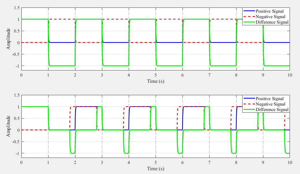
In the bottom subplot of Figure 7, a skew equal to 40% of the clock period is applied. This phase shift causes the positive and negative waveforms to fall so far out of alignment that they become almost completely in-phase again. Consequently, when the receiver subtracts them, the resulting difference signal cancels out almost entirely, surging away from 0 V for only a brief 20% interval of the clock period.
If skew reaches exactly 50% of the clock period, the complementary lines fall perfectly in-phase. When the receiver subtracts these identical waveforms, they cancel out completely across the entire timeline. Consequently, the differential output drops to a constant 0 V, resulting in complete signal destruction where no clock transitions can be recovered.
In the frequency domain, this destructive cancellation manifests as a notch-filter-like behavior in the SDD21 insertion loss plot. Put simply, SDD21 measures how much of your high-speed differential signal successfully travels from the beginning of the PCB trace to the end, and how much is lost along the way. At the specific frequency where the accumulated timing skew over a given line length equals exactly half the signal period, the signal undergoes total cancellation, creating a sharp, deep drop in transmission known as a resonance dip. Figure 8 shows the simulated differential insertion loss for a path with 65.2 ps of skew, which causes the resonant frequency null to appear at approximately 7.8 GHz.
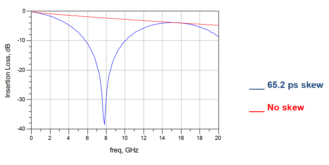
Since signal cancellation occurs when the skew equals half the signal period, the resonant null frequency is:
\[f_0 = \frac{1}{2 \times \Delta t_{skew}}\]
Equation 3
Note that S-parameters are defined using sinusoidal waves; however, the clock signal waveform was used in this section as an illustrative example to explain how skew drives the cancellation mechanism.
Conclusion: What This Means for Layout, and What Comes Next
Substrate non-homogeneity inherently causes variations in the propagation velocity of electromagnetic waves. This phenomenon results in an intra-pair timing skew that accumulates linearly down the path, systematically collapsing eye diagram margins and forcing deep SDD21 insertion loss nulls. While this installment focused on the underlying “why” behind laminate-induced signal integrity degradation, identifying the problem is only half the battle. The subsequent installments of this three-part series will explore the “so what,” presenting a practical framework of mitigation strategies, layout rules, and material choices to neutralize the fiber-weave effect in real-world designs.
Related Reading
Part 1: Understanding Fiber Weave Effect: From Glass Weave to Differential Skew (this article)
Part 2: Fiber Weave Skew Modeling: Analytical Bounds and Statistical Skew Prediction
Part 3: Mitigating Fiber Weave Skew, from Spread Glass to Routing Angle (coming soon)
Frequently Asked Questions
What is the fiber weave effect in a PCB?
The fiber weave effect is the timing mismatch that occurs when the two traces of a differential pair travel over different mixtures of glass and resin inside a PCB laminate. Glass bundles have a dielectric constant near 6 and the resin between them near 3, so signals over glass propagate slower. The resulting intra-pair skew accumulates with trace length and degrades differential signal quality.
What causes intra-pair skew on a matched differential pair?
Length matching equalizes the copper, not the material beneath it. Two traces routed to identical lengths can still accumulate significant skew if one sits predominantly over glass bundles and the other over resin-rich windows. Because the dielectric constants differ by roughly a factor of two, the propagation velocities differ by roughly 29%, and that difference is invisible to a length-matching check.
At what point does the fiber weave effect start to matter?
It becomes a design constraint when accumulated skew consumes a meaningful fraction of the unit interval, which depends on both data rate and trace length. Skew subtracts almost directly from the horizontal eye opening, so 0.2 UI of skew costs roughly 20% of the sampling window. Since skew accumulates linearly with length, long backplane, DDR, and PCIe runs hit the limit first.
How does fiber weave skew affect the eye diagram?
Intra-pair skew reduces the horizontal eye opening by approximately the skew amount. In the MATLAB model in this article, 0.4 UI of skew reduces a full 1 UI eye to roughly 0.6 UI, with finite rise and fall times cutting into both horizontal and vertical margin further. During the skew interval the difference signal sits at 0 V, so the receiver cannot resolve a logic high or low.
What causes resonance dips in an SDD21 insertion loss plot?
A resonance dip appears at the frequency where accumulated intra-pair skew equals exactly half the signal period. At that point the complementary waveforms arrive in phase, the receiver’s subtraction cancels them completely, and transmission collapses. The first null falls at f = 1 / (2 × skew), with additional nulls at odd multiples of that frequency. For example, 100 ps of skew places the first null at 5 GHz.
Is the fiber weave effect the same as the glass weave effect?
Yes. “Fiber weave effect,” “glass weave effect,” and “glass weave skew” all describe the same phenomenon: propagation velocity variation caused by the non-uniform distribution of glass and resin in a PCB laminate.
References
Nittobo. 2026. “Glass Cloth for Electronic Materials.” Electronic Materials Business, Business and Products. Accessed July 30, 2026. https://www.nittobo.co.jp/eng/business/electronicmaterials/pcbcloth/index.htm.
Simonovich, Lambert. 2011. “Practical Fiber Weave Effect Modeling.” White Paper, Issue 2. LAMSIM Enterprises Inc., January 10. http://www.lamsimenterprises.com/Practical_Fiber_Weave_Modeling_Iss2_Jan10-11.pdf.


.webp)