


Read the Full Series
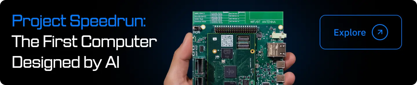
This article is one part of a walkthrough detailing how we recreated an NXP i.MX 8M Mini–based computer using Quilter’s physics-driven layout automation.
If you’ve ever run a traditional autorouter on a complex PCB, you know the frustration: tangled traces, odd detours, and hours spent cleaning up what was supposed to be “automatic.” But what if your design tool could actually think like an expert engineer? In this post, we’ll break down the real differences between old-school autorouting and the new wave of AI-powered PCB layout so you can choose the right tool for your next project.
Along the way, we’ll connect the dots to the search question many teams are really asking: what are the top rated automated circuit board design tools, and what kind of “automation” do they actually mean? Industry rankings often score full EDA suites on workflow coverage, collaboration, libraries, scalability, and cost. That matters, but it also hides a key detail: an autorouter is just one algorithmic feature inside a broader tool, while AI PCB layout can act like a full layout engine that generates, evaluates, and iterates complete designs.
Let's define what traditional autorouting actually does
Traditional autorouting is a path-finding approach that tries to connect nets automatically after placement, usually one connection at a time, while obeying a set of geometric and design-rule constraints. In most EDA tools, you give the router a board outline, a placement, and a set of rules, then it attempts to finish unrouted connections with minimal human involvement.
At a practical level, most autorouters work like this:
- They model the routable area as a grid or graph with obstacles (components, keepouts, existing copper).
- They search for valid paths between pins using strategies like maze routing, line-probe routing, or gridless routing.
- When they get stuck, many flows rely on iterative “rip-up and reroute” to remove earlier traces and try again with different priorities.
A classic example is maze routing (often associated with the Lee algorithm family): the router expands outward through the available space until it reaches the target, then backtraces a path. This can guarantee a shortest path in the simplified grid model, but it can be slow and memory-heavy, and it does not automatically capture higher-level design intent.
Why did autorouters become a staple? Because they can be useful on simple or repetitive routing tasks, and nearly every major PCB suite includes some form of automated routing or auto-interactive routing as part of the workflow.
Why do autorouters so often fall short?
Autorouters fall short because routing a real PCB is not just “connect A to B.” It’s a multi-objective optimization problem that involves physics, manufacturability, and design intent, all under tight geometric constraints. Traditional routers are strongest when the problem is cleanly constrained and “mostly geometric,” and they struggle when the board is dense, high-speed, mixed-signal, or has nuanced constraints that live in an engineer’s head.
Here are the most common real-world failure modes teams run into:
1) They optimize locally, not holistically
Many autorouters make decisions net-by-net or region-by-region. Even with global routing stages, the system often commits to early routes that block future critical paths, then tries to recover with rip-up and reroute. That recovery works sometimes, but it can also create a “spaghetti cleanup” outcome where you spend hours undoing what the tool did automatically.
2) They produce “legal” geometry that still looks wrong
A route can pass DRC and still be a bad layout. Classic symptoms include:
- unnecessary vias and layer swaps
- long detours that increase loop area
- awkward neck-downs near pins
- odd jogs that a human would never choose
These patterns show up because the algorithm is trying to solve a constrained puzzle, not express a clean electrical strategy.
3) Dense boards expose the limits of grid and search assumptions
Maze and grid-based approaches can become computationally expensive and brittle as density rises. The search space explodes, and the tool either times out, fails to complete, or completes in a way that is technically connected but practically unhelpful.
4) “Auto” often means “auto-first-pass,” not “auto-finished”
In many professional teams, autorouting is used selectively (or avoided) in favor of interactive routing, where the designer steers the path and the tool enforces rules. That hybrid approach exists for a reason: fully automatic routing rarely matches the combination of clarity, intent, and constraint awareness that an expert layout engineer delivers.
Here's how AI changes the game for PCB layout
AI-powered PCB layout changes the problem from “route these remaining nets” to “generate complete candidate layouts that satisfy constraints, then evaluate them against physics-aware checks.” Instead of treating routing as a late-stage patch, AI layout engines can treat the board as a system and optimize placement and routing together, repeatedly, until the candidates converge on workable solutions.
Quilter positions itself in that newer category: a physics-driven AI that automates complete PCB layout and produces multiple candidates in hours, while keeping you in your existing CAD workflow.
What’s fundamentally different from an autorouter?
1) The unit of work is the whole design, not a single trace
An autorouter is typically invoked to finish routing after placement, or to route a subset of nets. AI layout is closer to a “layout engineer in software” that can generate full candidates end-to-end, so you can review options instead of wrestling with one fragile routing run.
Quilter’s workflow emphasizes: upload native CAD projects, define board outline and constraints, generate candidates, then do transparent review before handoff back into your CAD tools.
2) Constraints and physics move from “afterthought” to “first-class inputs”
Traditional routing is good at geometry plus DRC. But modern boards care about things like impedance-controlled nets, differential pairs, bypass placement intent, return path continuity, manufacturability, and clean escape strategies.
Quilter explicitly markets physics-aware design considerations like bypass capacitors, impedance-controlled nets, and differential pairs, and it pairs generation with a design review layer that shows what is and is not accounted for.
3) Iteration is the product
One of the biggest practical advantages of AI PCB layout is not that it makes one “perfect” board instantly. It’s that it makes many good candidates quickly, so you can explore tradeoffs (stackups, form factors, component constraints, manufacturing assumptions) without burning calendar time. Quilter highlights this “iterate more” value directly as part of its positioning.
What results can you expect from AI-powered PCB design?
In practice, AI-powered PCB design should reduce the “layout bottleneck” by improving first-pass completeness and cutting manual cleanup, while making it easier to explore more design options in the same schedule. That is the core outcome teams care about when they search for automated circuit board design tools: not “does it draw lines,” but “does it help me ship hardware faster with less risk.”
Quilter’s public positioning is built around compressing layout time and enabling rapid iteration, with outputs returned in the same CAD formats so teams can run their normal DRC and release processes.
Here’s what “better results” usually looks like, in measurable and reviewable terms:
Higher completion with fewer ugly surprises
Traditional autorouters can connect a lot of nets, but completion is not the only metric. AI layout aims to deliver candidates that look and behave more like expert layouts: coherent routing strategy, fewer unnecessary vias, cleaner escape patterns, and fewer manufacturing red flags.
Quilter also publishes comparisons focused on efficiency and outcomes across tools, framed as side-by-side testing (Quilter vs traditional PCB tools). Use these as internal supporting assets, and pair them with third-party sources for credibility.
Less manual rework before manufacturing
The expensive part of “automation that fails” is the cleanup: rerouting critical nets, redoing plane strategy, fixing neck-downs, untangling returns, and restoring readability. AI layout’s value is that it can front-load more of that quality, so your manual work shifts toward review and refinement instead of rescue.
Faster iteration loops and better trade studies
An EEJournal feature on AI-powered PCB layout describes the broader industry trend as enabling teams to explore the solution space more effectively when time and cost compress. That aligns with the “generate many candidates, choose the best” model that AI layout tools emphasize.
How do you choose the right automated PCB design tool?
Choose based on what you actually need automated: routing assistance, workflow acceleration, or end-to-end layout generation with physics-aware review. Many “top rated” lists rank complete EDA environments, not the quality of one autorouter run. So the right decision framework is: what level of automation reduces my current bottleneck without breaking my process?
Step 1: Understand what “top rated” often means
Recent comparisons and roundups score PCB tools on factors like workflow coverage, collaboration, libraries, scalability, and cost. Those are valid criteria for selecting a primary CAD environment. For example, EMA’s rankings publish weighted scoring tables and often place enterprise suites like Allegro X, OrCAD X, and Altium Designer near the top, with KiCad and EasyEDA scoring strongly on accessibility and cost.
That answers: “What is a top rated PCB design suite?”
It does not fully answer: “What will remove my PCB layout bottleneck?”
Step 2: Map your project to the right automation level
Use this quick comparison table to self-identify where you fit.
What you need
Best fit
Why it works
Where it breaks
Simple 2-layer boards, low density
Traditional autorouter
Fast enough for straightforward connectivity
Cleanup can still cost more than it saves
Dense routing, but designer wants control
Auto-interactive routing
Designer steers intent, tool enforces rules
Still depends on expert time and skill
Fast layout cycles, many iterations, constraint-heavy boards
AI PCB layout
Generates full candidates, supports review and selection
You still need engineering review and sign-off
Auto-interactive routing is widely described as “designer-guided automation” rather than full autorouting, which is why many pros prefer it for quality control.
Step 3: Evaluate tool fit using a checklist
Checklist: picking the right automation approach
- Board complexity: Is this high-speed, dense, or mixed-signal? If yes, pure autorouting is less likely to deliver clean results.
- Constraint maturity: Do you have clear design rules and constraints defined? Any automation needs good constraints, and AI benefits from explicit intent.
- Iteration pressure: Are you schedule-bound and need multiple layout candidates quickly? AI layout is strongest when iteration is the constraint.
- Team bandwidth: Are layout engineers a bottleneck? AI can increase engineering bandwidth by shifting effort from manual routing to review and refinement.
- Workflow compatibility: Do you need to stay in Altium, Cadence, Siemens, or KiCad? Quilter emphasizes working with existing workflows and returning files in the same format for handoff.
- Security and support needs: If you are in a mission-critical environment, support and operational maturity matter as much as features. Quilter highlights enterprise-grade support and secure engagement models.
A practical way to benchmark AI PCB layout tools
When you trial AI PCB layout (Quilter or any alternative), use a repeatable test:
- Pick a board you know well (or a representative block).
- Lock only the constraints you truly need (connectors, keepouts, critical placement anchors).
- Generate multiple candidates.
- Compare: via count, unrouted nets, critical path length, manufacturability flags, readability.
- Measure how long it takes you to get to “fab-ready confidence.”
This gives you a real answer to “top rated automated circuit board design tools” for your work, not just an abstract ranking.
Next steps: Getting started with Quilter’s AI layout
The fastest way to understand the autorouter vs AI difference is to run the same design through both and compare candidates side-by-side. Quilter offers an always-free tier designed to let teams generate layouts and iterate without manual routing, and it positions pricing around usage rather than seats.
Here’s a straightforward path to get moving:
- Start with the Product Overview to understand the workflow: upload native CAD projects, define constraints, generate candidates, review, then hand off back to your CAD tools.
- Try the free version with a representative board to see how candidate generation and review feel in your process.
- Use the documentation and Help Center to answer common evaluation questions like supported CAD formats, how Quilter works, and how it differs from an autorouter.
- If you need a higher-touch rollout, explore support options designed for mission-critical environments.
Ready to see the difference? Try Quilter’s AI-powered PCB layout for free or schedule a live demo with our engineering team.
Top rated automated circuit board design tools and what they’re best at
If you’re evaluating the landscape, it helps to separate “primary CAD suite rankings” from “layout automation capability.”
- Top-rated suites (workflow + enterprise features): Allegro X, OrCAD X, Altium Designer frequently score highly in weighted comparisons focused on enterprise workflow factors.
- Accessible and cost-effective suites: KiCad and EasyEDA often rank strongly on accessibility and cost, with varying strengths in routing workflows depending on your constraints.
- AI PCB layout tools: Industry coverage notes a growing set of AI-powered layout products emerging since late 2024, including Quilter among others.
The right move is not picking a “winner.” It’s matching the automation type to your bottleneck, then validating it on your own design with a measurable comparison.


