


Read the Full Series
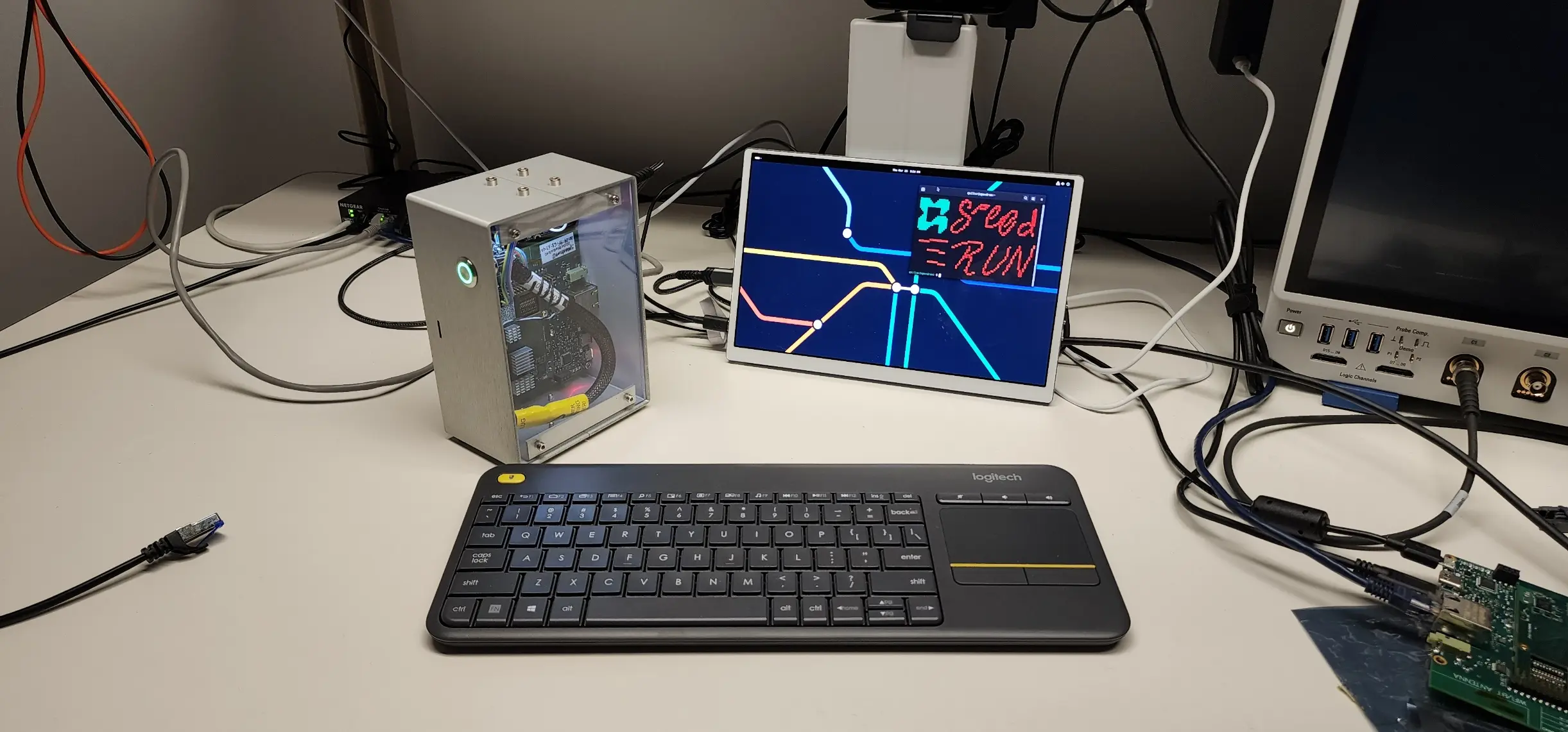
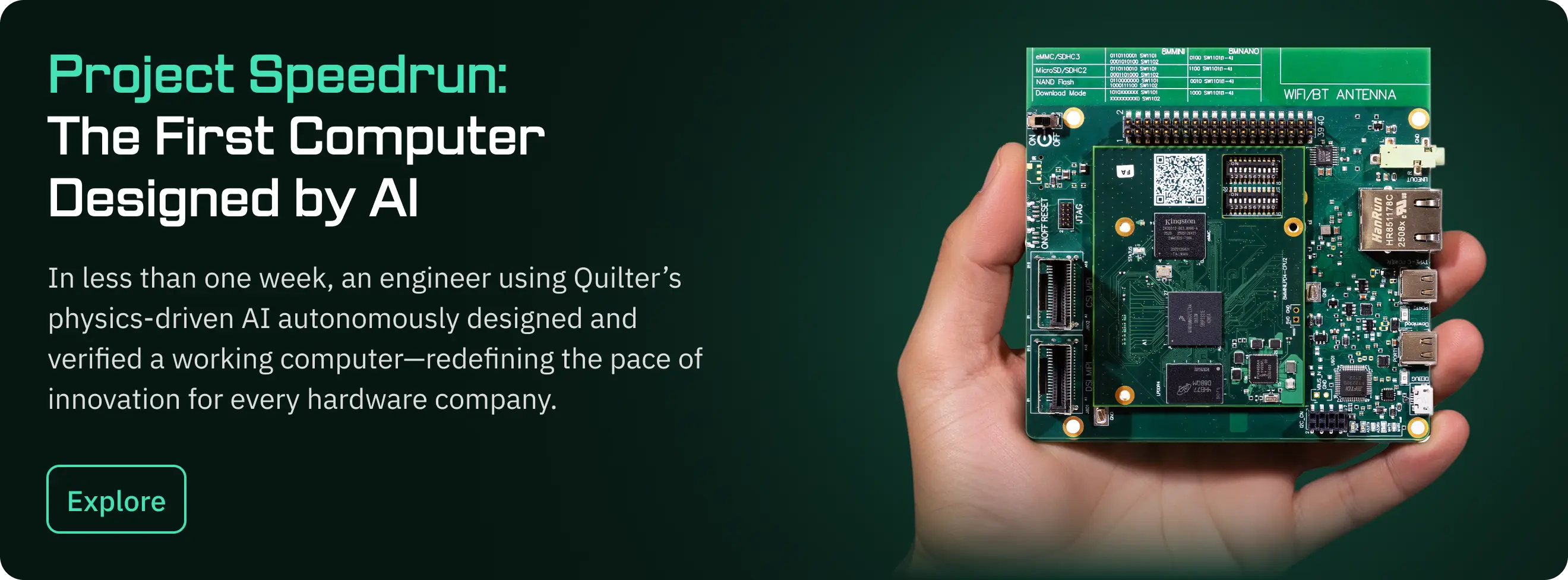
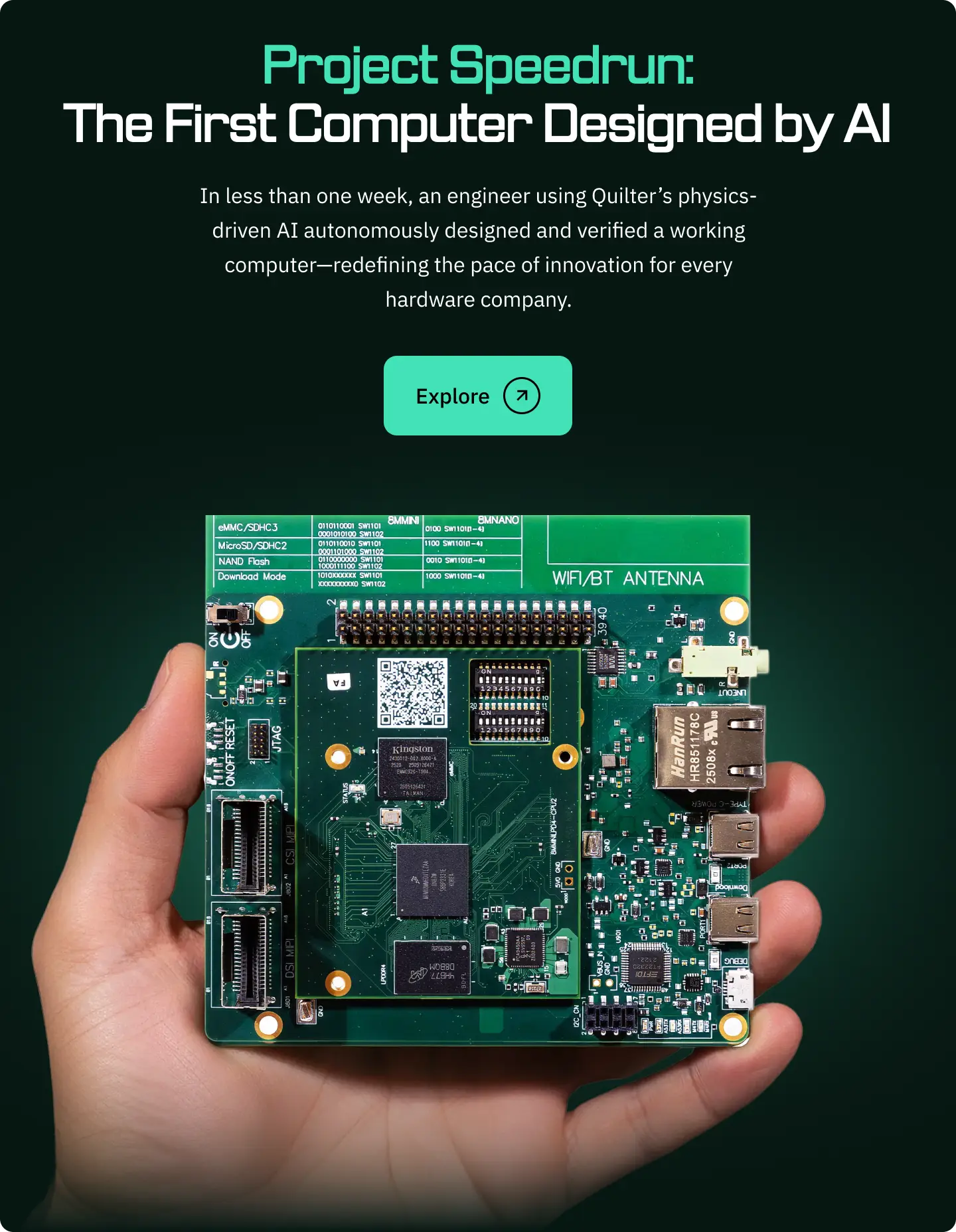
This article is one part of a walkthrough detailing how we recreated an NXP i.MX 8M Mini–based computer using Quilter’s physics-driven layout automation.
The tools you use to design hardware in 2026 do not look much like the CAD stacks most teams were trained on. The old model was linear. Capture the schematic, hand the design to layout, wait on routing, discover problems late, then scramble through revisions. That workflow still exists, but it is being pressured from every direction at once. Boards are denser. Timelines are tighter. Mechanical, electrical, and manufacturing constraints collide earlier. And more teams are realizing that they cannot hit modern product schedules if PCB layout remains a week-long bottleneck.
That pressure is why innovative hardware design platforms are getting real attention now. The most important shift is not simply that hardware tools are moving to the cloud. It is that AI is moving upstream from assistance to generation. The new class of tools does not just help engineers place traces faster. It generates candidates, scores tradeoffs, surfaces constraint issues, and makes iteration abundant rather than scarce. At the same time, system-level simulation vendors are tying electronics and physics together more closely, while cloud-native mechanical platforms are making collaboration and model sharing feel less like a handoff and more like a shared workspace.
For teams building complex electronics, that changes the question. It is no longer “Which CAD seat should we buy?” It is “Which stack lets us explore more valid designs, with more confidence, without breaking the workflow we already trust?” Quilter sits squarely inside that answer. According to Quilter’s product and solutions messaging, the company is focused on reinforcement learning for PCB layout, physics-aware review, native ECAD compatibility, and turning schematic-to-fab-ready work from weeks into hours.
Let’s define what’s really changing in hardware design right now
Three things are changing at once.
First, hardware design is becoming computationally richer. In the old flow, engineers used software to draw and check. In the new flow, software is expected to generate, evaluate, and propose. That is a bigger change than interface modernization. It means the tool is no longer just a drafting environment. It becomes an active design participant.
Second, the stack is becoming more connected. PCB, enclosure, manufacturing, and simulation are no longer separate conversations that happen in sequence. Fusion now positions itself as an integrated cloud platform spanning CAD, CAM, CAE, PCB, and data management. Onshape continues to push cloud-native collaboration and built-in data management as core workflow features, not add-ons. Synopsys is explicitly framing its Ansys acquisition as a silicon-to-systems play that unifies electronics and physics.
Third, teams are under market pressure to iterate more before committing. That is especially true in semiconductors, robotics, aerospace, and consumer electronics, where board delays can cascade into missed validation windows, missed tape-out schedules, or missed launch dates. Quilter’s own positioning leans into exactly that pressure: more candidate boards, earlier in the program, with physics review layered into the workflow.
This is the real backdrop for Hardware Design 2026. It is not hype about AI for its own sake. It is a search for engineering bandwidth.
Here’s how AI-native platforms are reshaping PCB layout
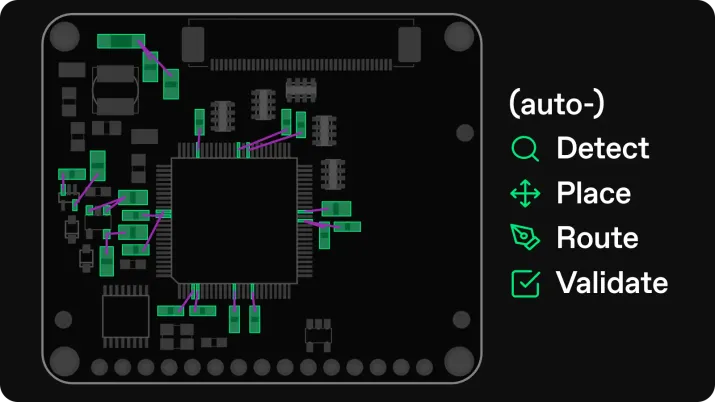
AI-native PCB design differs from traditional automation because it is not limited to a single narrow step. The older automation mindset focused on faster routing, rules checking, or guided suggestions. The newer model is generative. The system explores full-board candidates, scores them against constraints, and gives engineers multiple viable directions to review.
That broader shift is visible across the category. Flux presents itself as a browser-based ECAD platform with AI embedded into the design workflow. Diode positions itself at the forefront of AI-driven board design and manufacturing. Those are signals that the market is moving from “EDA with a few smart helpers” toward “platforms where AI is a primary design surface.”
Quilter’s angle is more specific and more technically relevant for serious teams. Based on the company context you provided, Quilter uses reinforcement learning to explore large design spaces, generates multiple layout candidates in hours, and runs a physics-aware review that covers issues like bypass capacitors, impedance-controlled nets, and differential pairs. It also returns projects in the same ECAD format teams already use, including Altium, Cadence, Siemens, and KiCad. That matters because most engineering organizations do not want novelty at the expense of handoff risk. They want more layout throughput without tearing up the rest of the toolchain.
The workflow implication is big. PCB designers move from manually pushing every trace to shaping constraints, curating candidates, and reviewing results at a higher leverage point. R&D managers get faster board bring-up. Electrical engineers get schematic-to-board cycles in hours rather than waiting in a serial queue. Quilter’s own positioning claims that first candidates often appear within the first hour, and full fab-ready designs can be delivered in under four hours for supported use cases.
What changes with physics-first AI?
- Multiple board candidates in hours
- Review artifacts tied to physical constraints, not just aesthetic layout preferences
What you need to know about system-level AI co-design
System-level co-design is the idea that electronics, mechanics, thermal behavior, manufacturability, and sometimes firmware assumptions should be evaluated together, not in disconnected phases. In practice, that does not mean one giant magical tool will replace the entire stack. It means the best platforms will share constraints, results, and tradeoffs across domains.
You can see the direction clearly in the Synopsys and Ansys story. Synopsys says the combination is aimed at deeper integration of electronics, physics, and AI-driven insights across silicon and systems. That is exactly the kind of stack-level convergence hardware teams have been asking for, especially in products where PCB decisions are inseparable from thermal, mechanical, and signal-integrity realities.
At the board level, physics-driven PCB design is a prerequisite for that future. A co-design workflow is only useful if the board tool can reason about real electrical constraints rather than just geometric legality. That is where Quilter’s positioning fits cleanly. If a robotics team wants to compare multiple stack-ups, multiple form factors, and multiple board candidates while preserving core electrical constraints, then a physics-aware layout engine becomes a building block for system-level AI co-design, not just a routing convenience.
The more realistic view is this: co-design in 2026 is an ecosystem problem. You need simulation depth, layout automation, mechanical collaboration, and clean handoffs. The winners will not be the flashiest monoliths. They will be the platforms that share truth well.
How are chips, boards, and enclosures starting to converge?
The hardware stack is getting stitched together from both ends.
At the silicon layer, OpenROAD continues to push an autonomous RTL-to-GDS flow aimed at lowering the cost, expertise burden, and risk of chip implementation. Its mission is explicitly tied to democratizing hardware design through automation. That does not make OpenROAD a PCB tool, of course, but it does make it part of the same broader story: more of the design stack is becoming programmatic, automated, and cloud-coordinated.
At the enclosure and product-geometry layer, bitbybit.dev offers browser-based parametric CAD and configurator workflows, while Onshape and Autodesk Fusion continue to advance cloud-native collaboration and integrated product-development environments. In other words, even outside PCB layout, the center of gravity is moving toward shared models, browser access, and fewer brittle file-based handoffs.
Forward-leaning teams are already thinking this way. They may evaluate chip blocks in automated IC flows, generate board candidates in Quilter, validate fit with cloud MCAD, and coordinate revisions without treating each domain as a sealed-off department. The key requirement is interoperability. A board respin should not blow up the enclosure model. A mechanical change should not get lost before the layout team sees it.
That is why Quilter’s compatibility message matters. If the system fits into existing ECAD flows and returns native-format outputs, it can serve as the PCB automation layer inside a larger modern stack rather than forcing a full-stack replacement.
Simple diagram: where Quilter fits in the modern hardware stack
Schematic / Constraints
↓
Quilter AI PCB Layout Layer
- candidate generation
- physics-aware review
- native ECAD handoff
↓
Simulation / Validation
↓
MCAD / enclosure tools
↓
Manufacturing / supply-chain / DFM
Here’s why supply-chain-aware design is becoming table stakes
A fast design that cannot be sourced is not a fast design. It is a detour.
That is why AI-verified supply chain thinking is becoming part of the platform conversation. Flux, for example, emphasizes live parts data within its browser-based workflow. Autodesk Fusion also frames electronics and manufacturing in a more connected product-development context. The direction is clear: design systems are being asked to reason not only about geometry and rules, but also about what can actually be built.
The next logical step is obvious. Candidate generation and candidate scoring should incorporate component availability, lifecycle risk, second-source options, and manufacturing realities. Quilter’s physics-first approach does not, by itself, solve supply chain exposure. But it fits naturally into a workflow where physics-valid board candidates are paired with live sourcing intelligence so teams do not waste time polishing layouts built around fragile BOM assumptions. That is an inference, but it is grounded in where these platforms are heading.
For validation boards, test fixtures, and export-sensitive programs, this matters even more. The useful future is not “AI made me a board fast.” The useful future is “AI made me a board fast, and it is still buildable under real constraints.”
What results can real teams expect from physics-first AI?
This is where the category stops being abstract.
Based on Quilter’s own messaging, the company is targeting concrete outcomes across several board types: test fixtures and harnesses can shave four to six weeks off board bring-up, IC evaluation boards move from weeks to hours, design validation boards shrink validation cycles from months to days, and backplane or interconnect work can go from 30-plus days to under 24 hours. The company also claims first candidates often appear within the first hour, with full fab-ready designs in under four hours for supported workflows.
The industry framing is equally specific. Semiconductor teams care about validation speed and tape-out support. Aerospace and defense teams care about cutting delays while respecting MIL-STD and ITAR-sensitive environments. Consumer electronics teams care about hitting market windows without layout bottlenecks. Robotics teams care about compressing bring-up and testing cycles. Those are not generic productivity claims. They are workflow and schedule claims.
The qualitative upside may be even more important than the headline speed. More candidate boards mean more design-space coverage. More rapid constraint feedback means fewer late-stage surprises. And a transparent physics review gives engineers a clearer picture of what the AI has handled well versus what still needs human judgment. That last point matters. Trust in AI hardware design will not come from magic. It will come from honest visibility.
Quilter outcomes highlighted on site
- Test fixtures and harnesses: 4 to 6 weeks off bring-up
- Backplanes and interconnects: 30-plus days to under 24 hours
Here’s how to evaluate innovative hardware platforms in 2026
Do not evaluate these platforms solely on demo polish. Evaluate them the way you would evaluate any engineering tool that might end up on the critical path.
Start with five questions. How deep is the physics reasoning? How well does it fit the ECAD and MCAD tools you already trust? How much supply-chain awareness is present today? What governance and compliance posture exists for sensitive programs? And how is pricing aligned with actual usage? Quilter’s brief, for example, emphasizes native-tool compatibility and pin-count-based pricing rather than seat-based pricing, which is a very different operating model from traditional EDA procurement.
Then run a live test. Pick a real board from your backlog, ideally one with moderate complexity and clear success criteria, such as a test fixture or validation board. Measure time to first candidate. Measure time to a fab-ready output that your team would actually sign off on. Ask what the AI explicitly checks and what it does not. Ask for review artifacts, pass-fail breakdowns, and anything that ties the recommendation back to a physical model.
That is also how to place the broader market. OpenROAD belongs in the chip-automation conversation. Synopsys and Ansys belong in the system simulation and silicon-to-systems conversation. Cloud MCAD belongs in the collaboration and geometry conversation. Quilter belongs in the physics-driven layer of PCB layout automation. The strongest stack may include all of them, but each solves a different bottleneck.
Where Quilter fits in the future hardware stack
Quilter is best understood as the physics-driven board layout engine in a modern hardware toolchain.
It sits after schematic and constraint definition, before final signoff and manufacturing output. That is exactly where many teams still experience the most painful serial delays. According to the company brief, Quilter imports and exports native projects from major ECAD environments, explores multiple layout options with reinforcement learning, performs transparent physics-aware design review, and returns results in the same format teams already use for DRC, polish, and fab generation.
In prose, the stack looks like this: chip and silicon exploration in tools such as OpenROAD or commercial IC flows; board implementation and candidate generation in Quilter; enclosure and mechanical coordination in Onshape, Fusion, or a parametric browser CAD; then manufacturing and supply-chain systems layered on top. That is a cleaner way to think about innovative hardware design platforms than to pretend that one vendor will own every inch of the workflow.
For R&D managers, Quilter is a schedule accelerator. For PCB designers, it is a way to focus human judgment on the most challenging parts of the board rather than spending cycles on repetitive layout work. For electrical engineers, it shortens the distance between circuit intent and a board on the desk. That positioning is consistent across the company context you shared.
What’s next for hardware teams that adopt these tools?
The likely future is not fewer boards. It is more boards, earlier, with better information attached to each one.
That is what hardware-rich development looks like in practice. Teams move from rationing iteration to planning around it. They stop treating layout as a narrow downstream task and start treating it as a high-bandwidth design loop. Some of those loops will still fail, of course. Good engineering always includes dead ends. But the cost of exploring them drops.
The smart next step is not a giant platform migration. It is a bounded pilot. Take one low-risk but useful design, such as a test fixture, harness board, or validation board. Define the constraints clearly. Run it through a physics-driven AI PCB layout flow. Compare the outputs against your current process. Then turn what you learn into an operating checklist so this becomes a repeatable workflow rather than a one-off experiment. That recommendation aligns with the implementation goals in your brief and with Quilter’s own adoption framing.
For teams actively comparing innovative hardware design platforms in 2026, that is the practical takeaway. Look for platforms that give you more design cycles, clearer physics visibility, cleaner handoffs, and less wasted iteration. Quilter is not the whole stack. It does not need to be. Its role is to make PCB layout fast, abundant, and physics-aware enough that the rest of the stack can move faster too.
Run your next test fixture through Quilter, compare time-to-fab-ready against your current flow, and use that pilot to decide where physics-driven AI belongs in your hardware stack.