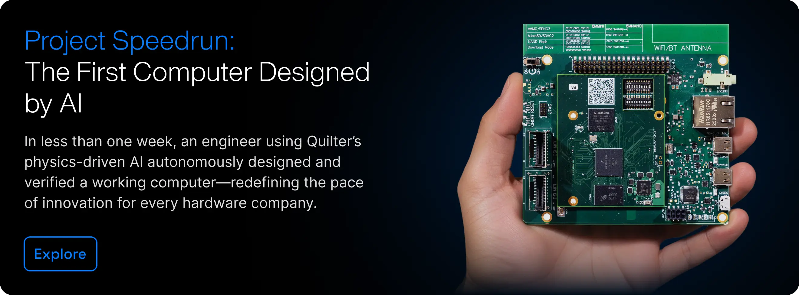
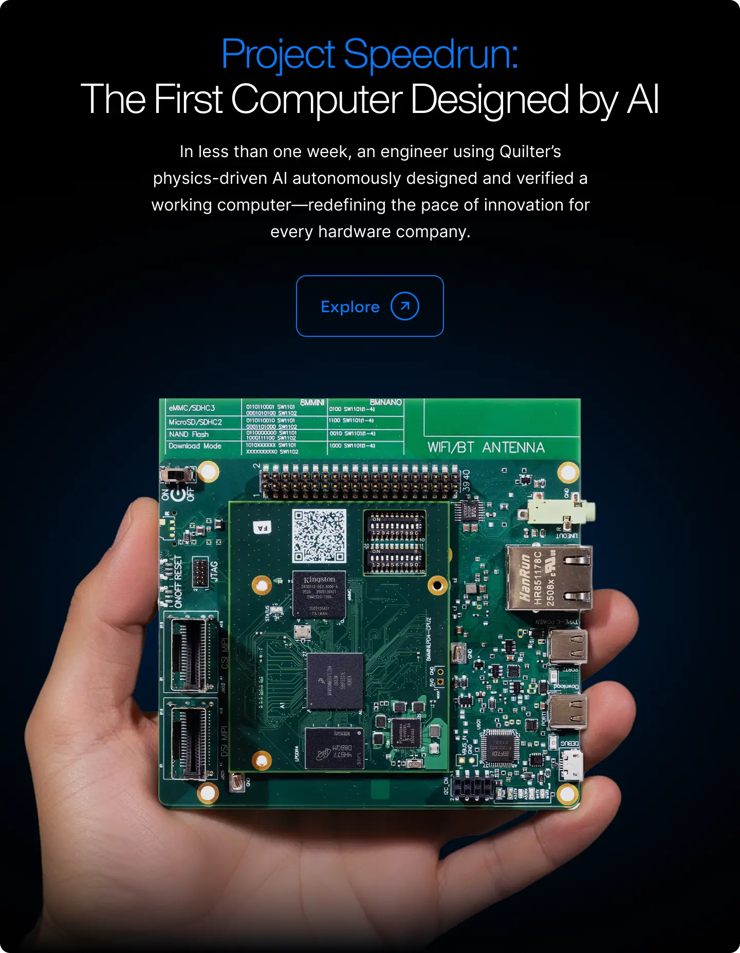


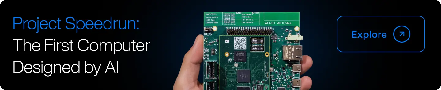


Read the Full Series
This article is one part of a walkthrough detailing how we recreated an NXP i.MX 8M Mini–based computer using Quilter’s physics-driven layout automation.
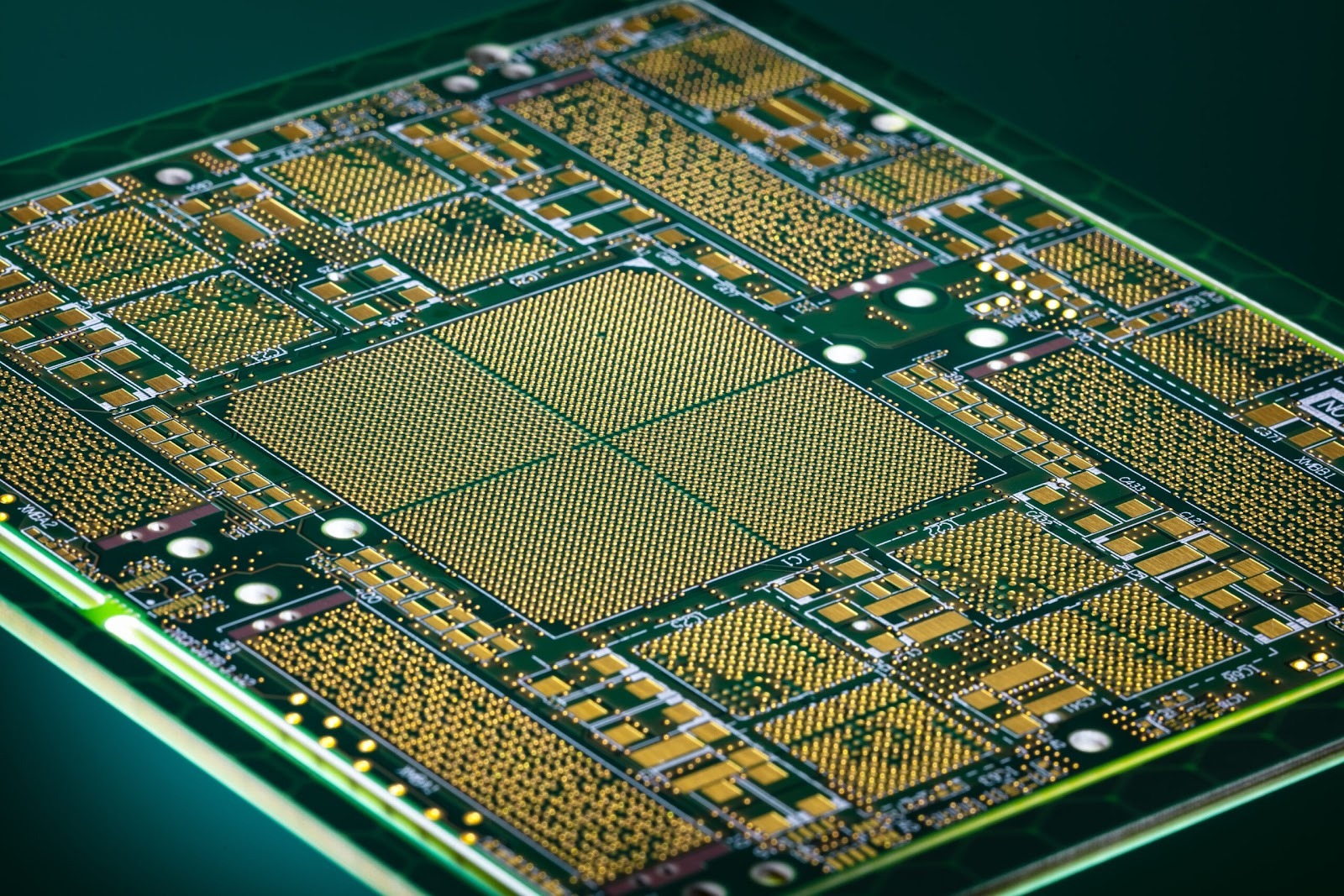
Dense BGAs are the ultimate stress test for any PCB layout workflow. When a high-pin-count device hits your stackup, you instantly feel the weight of via congestion, layer pressure, impedance demands, and the risk of a single misrouted escape dictating your entire floorplan. In this case study, we show how Quilter AI handled a 1200-pin FPGA BGA and produced a DRC-clean layout in hours, not weeks. If you work with complex digital, RF, or mixed-signal boards, this deep dive will show exactly what next-generation automation can deliver.
What Makes Dense BGAs So Challenging?
Dense BGAs create an exponential routing problem. Every ball in the grid is a constraint that interacts with dozens of others. Once pin counts rise above 800 or pitches shrink below 0.8 mm, manual routing becomes a slow grind that depends on designer intuition and trial-and-error iteration.
Traditional EDA autorouters struggle for a few core reasons:
- Escape routing grows non-linearly
Routing the first 100 pins is easy, but the last 20 often dictate whether the board fails DRC or forces an extra layer. - Via congestion becomes the bottleneck
Even small inefficiencies compound when hundreds of pins compete for the same routing channels. - SI and EMI rules create hard constraints
A single misrouted differential pair or poorly placed bypass capacitor can invalidate an entire fanout strategy. - Manual iteration is slow and brittle
Designers usually fan out manually, massage escape routes by hand, and adjust layer assignments until the board converges. This process often consumes 3 to 6 weeks for a single high-pin-count FPGA.
Because of this complexity, dense BGAs highlight the limits of traditional workflows and create an ideal proving ground for physics-aware, AI-driven routing.
How Did We Approach a 1200-Pin FPGA Layout?
This case study focuses on a real 1200-pin FPGA BGA with a 0.8 mm pitch placed near the center of a 14-layer board. The engineering team needed a deterministic, DRC-clean layout that met strict signal integrity and manufacturability requirements.
Key metrics
- 1200 BGA pins
- 0.8 mm pitch
- 14 layer stackup
- Differential pairs routed: 68
- High-speed nets: 220+
- Bypass capacitors: 52 around the device
- Target: Fully routed and DRC-clean in hours
The device pushed every classical bottleneck: escape routing pressure, via count restrictions, and tight impedance tolerances. The team also needed to preserve a fixed board outline and pre-placed high-speed connectors.
Initial Fanout Constraints
The engineering team uploaded their Altium project directly into Quilter. The FPGA and several connectors were already placed. The challenge was routing the full BGA breakout without violating impedance, length matching, or manufacturing constraints.
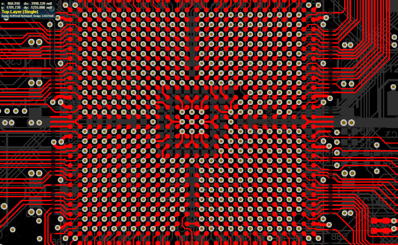
Below is the initial fanout inside Quilter.
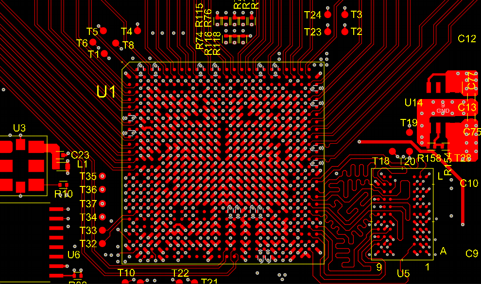
The design constraints were strict:
- Controlled impedance requirements on DDR and SERDES lanes
- Maximum via count per net
- Specific preferences for microvia usage
- Stackup locked to 14 layers
- Mandatory proximity guidelines for bypass capacitors
- Fabrication rules from a Tier 1 manufacturer
This is a representative challenge faced by semiconductor validation teams, aerospace programs, and high-density consumer electronics workflows every day.
What Steps Did Quilter AI Take - And Why?
Quilter uses a physics-driven reinforcement learning engine that evaluates millions of routing possibilities and converges on solutions that satisfy both electrical and manufacturing rules. For this design, the system followed a structured, explainable sequence that mirrors how an expert designer approaches the problem.
Step 1: AI-driven initial fanout
Quilter begins by identifying optimal escape vectors for each BGA row, choosing via patterns that minimize congestion and reduce the number of layers required for escape routes.
Why this matters:
Most autorouters treat each pin independently. Quilter treats the fanout as a global constraint-solving problem, balancing all escape routes simultaneously to avoid late-stage congestion.
Step 2: Escape routing with reinforcement learning
The engine explored thousands of escape patterns and selected the one with the lowest predicted via conflict density. The reinforcement learning model penalizes dead ends, unnecessary detours, and trace behavior that may cause SI degradation.
Key logic Quilter applied:
- Avoid dogbone patterns that create microvia clusters
- Lower layer-to-layer transitions unless electrically required
- Prioritize orthogonal routing symmetry for controllable impedance
- Keep high-speed lanes grouped and bundle them early
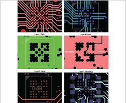
Step 3: Layer assignment and signal integrity compliance
Once escape routing was complete, Quilter mapped nets to layers using physics-based cost functions. These functions weigh impedance tolerance, coupling risk, and local via density.
Core inputs included:
- Manufacturer impedance tables
- Maximum allowed crosstalk coupling
- Differential pair spacing rules
- Ground reference continuity requirements
This ensures that routed nets are not only DRC-clean but also electrically compliant.
Step 4: Physics-driven constraint validation
Quilter ran a full physics validation pass on the design. This step checks bypass capacitor distances, trace lengths, impedance, shield continuity, and other signal integrity rules.
Every candidate route undergoes this validation before Quilter presents it to the user. That means engineers receive deterministic, compliant routing candidates rather than a messy autorouter dump.
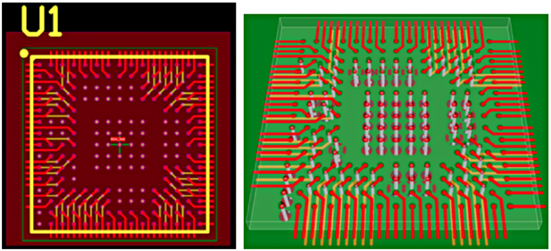
Step 5: Final polishing and DRC check
Quilter delivered a DRC-clean layout in approximately 2.5 hours. The engineering team reviewed the results in Altium and confirmed that every constraint was met.
No additional layers were required and the via count stayed within budget, two of the biggest wins for dense BGA routing.
Here’s How Quilter AI Compares to Other AI PCB Tools
To help engineers researching dense BGA automation, here is a direct comparison of Quilter AI versus other AI-enabled tools. The focus is specifically on dense BGA performance, not generic EDA features.
Dense BGA Automation Comparison Table
Key Takeaways
- Quilter handles the highest pin counts with the least user intervention.
- DeepPCB and TopoR are strong for mid-range BGAs but lack physics validation.
- Zuken CR-8000 offers sophisticated AI placement, but routing dense BGAs remains difficult.
- Altium provides powerful constraints but still depends heavily on manual iteration.
- OpenROAD is not optimized for PCB-level BGA routing.
If your workflow depends on deterministic routing of 800 to 1500 pin packages, Quilter is one of the few tools designed specifically for that density.
What Results Can You Expect From Automated Dense BGA Routing?
After running the full Quilter routing pipeline, the engineering team received a complete, production-ready layout. Below are the core metrics.
Final performance metrics
- Time to full DRC-clean routing: 2.5 hours
- Total via count: Reduced by 22 percent vs. manual baseline
- Escape routing completion success: 100 percent of pins escaped without rerouting
- Layer usage: All within 14 layer constraint
- Maximum trace length mismatch: Within 4 mil of targeted tolerance
- SI issues detected: 0 after validation
- Bypass capacitor proximity compliance: 100 percent
Before and after visualization

Practical implications
Engineers often spend weeks tuning a dense BGA breakout before routing the rest of the board. With Quilter, that entire step is automated, predictable, and repeatable. Teams can run multiple layout candidates, test different stackups, and compare manufacturability options in parallel.
This is especially valuable for:
- Semiconductor validation hardware
- Aerospace programs with strict EMI requirements
- High-density consumer electronics
- Rapid prototyping for R and D environments
- Teams struggling with PCB designer bandwidth
The result is not only faster time to first board but also higher reliability and fewer respins.
Ready to Accelerate Your Next Complex PCB Layout?
If your team is facing dense BGAs or multi-connector high-speed designs, Quilter AI can deliver deterministic, physics-driven layouts in hours. Upload your CAD files to try the workflow yourself or request a custom demo with one of our engineers.
- Learn more about the product: https://www.quilter.ai/product
- Explore documentation: https://docs.quilter.ai
- Request support: https://www.quilter.ai/support
- Contact our team: https://www.quilter.ai/contact
If you have questions about this case study or want to see additional examples, leave a comment or reach out to our engineering team.