Perfect, when delivered late, is worthless. Success belongs to the teams who ship early, learn fast, and keep momentum. To compete and lead on the global stage, speed is your competitive edge.
Too many of us still treat development as if it were a mini version of production. Same careful processes. Same sequential thinking. Same fear of failure. This mindset kills innovation before it takes root.
Hardware-rich development is the reset. Every fast, cheap cycle is an opportunity to surface risks, validate decisions, and unlock insights.. The next generation of hardware leaders are pulling ahead. Are you going to wait around to be outpaced?.
Dynamic hardware teams treat rapid iteration as a strategic advantage. The faster they learn from real-world prototypes, the faster they innovate, adapt, and ship.
Linear development is obsolete and clinging to its false sense of control is a liability.
Rapid iteration is now the baseline. Teams don’t waste days arguing with each other when they’re aligned from the start. Breakneck timelines are accomplished by using talents and resources instead of watching your competitors outpace and outperform you.
Experienced designers are essential to delivering production-ready hardware. Their expertise ensures stability, compliance, and quality where it matters most. But development is a different world—one that thrives on speed and exploration, not precision and certainty. This is where AI and automation help. With early-stage iteration offloaded, engineers can rapidly try—and discard—hundreds of design ideas without burdening the design team. That frees PCB designers and engineers to stay focused on what they do best: delivering innovation in real products for real-world deployment. AI protects their time and reserves their expertise for the work that defines careers—debugging complex systems, supporting high-value programs, and driving the critical decisions that shape what ships.
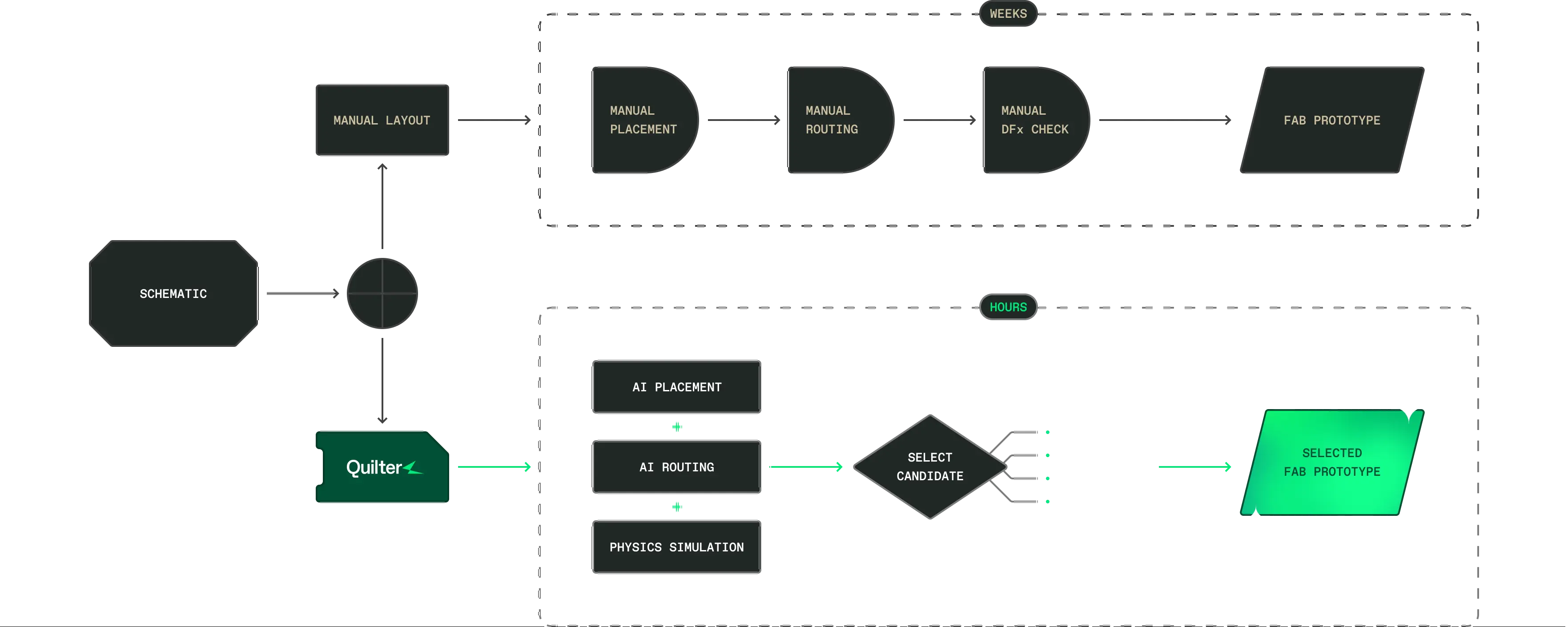
Quilter is a physics-driven layout engine that autonomously generates hundreds of fully placed, fully routed, constraint-checked design candidates from your circuits and constraints—refining every pass using reinforcement learning and physics-based rule checks. It’s not a co-pilot. It’s not a tool assist. And it’s definitely not an autorouter.
Physical boards surface the issues simulation misses. With real hardware on the bench in days, not weeks, your team gets more cycles, sharper insight, and faster time to market.
While PCB experts stay focused on production-grade programs, R&D teams finally get what they’ve always needed: a way to run hardware fast, iterative, and unconstrained.
Every delay widens the gap between idea and impact, between you and the team already on their second iteration. Competitors aren’t waiting for you.

Faster iteration means faster launches, more product shots, earlier market entry, and the confidence to lead on features, pricing, and adoption.

Teams stuck in bottlenecks bleed engineering hours, outsource unnecessarily, and trade agility for handoffs.

When iteration is slow, failure is expensive. But when it's fast, failure is just feedback. You find flaws earlier, fix them faster, and build confidence before you commit.
Design with Your Hands, Lead with Your Eyes — Nancy Smith and the Grounded Future of PCB Design
There’s no hierarchy. We all just want to build the best product.
Hardware-rich development
The Joy is the Job: Nancy Smith on Crafting Beautiful Hardware, One PCB at a Time
Most of us in engineering are chasing progress but beneath the metrics and milestones lies something quieter: happiness.
Hardware-rich development
Just Ship It: Lessons in Grit, Test, and Team from Paul Robinson’s Hardware Odyssey
That polymath tendency—the willingness to learn a bit of everything—is often the best preparation for a future no one can predict.
Hardware-rich development

Subscribe to the hardware-rich development newsletter